SLUSFS6
October 2024
TPS62A04AB
,
TPS62A04B
PRODUCTION DATA
1
1
Features
2
Applications
3
Description
4
Device Comparison Table
5
Pin Configuration and Functions
6
Specifications
6.1
Absolute Maximum Ratings
6.2
ESD Ratings
6.3
Recommended Operating Conditions
6.4
Thermal Information
6.5
Electrical Characteristics
6.6
Typical Characteristics
7
Detailed Description
7.1
Overview
7.2
Functional Block Diagram
7.3
Feature Description
7.3.1
Power Save Mode
7.3.2
100% Duty Cycle Low Dropout Operation
7.3.3
Soft Start
7.3.4
Switch Current Limit and Short-Circuit Protection (HICCUP)
7.3.5
Undervoltage Lockout
7.3.6
Thermal Shutdown
7.4
Device Functional Modes
7.4.1
Enable and Disable
7.4.2
Power Good
8
Application and Implementation
8.1
Application Information
8.2
Typical Application
8.2.1
Design Requirements
8.2.2
Detailed Design Procedure
8.2.2.1
Setting the Output Voltage
8.2.2.2
Feedforward Capacitor
8.2.2.3
Output Filter Design
8.2.2.4
Input and Output Capacitor Selection
8.2.3
Application Curves
8.3
Power Supply Recommendations
8.4
Layout
8.4.1
Layout Guidelines
8.4.2
Layout Example
9
Device and Documentation Support
9.1
Device Support
9.1.1
Third-Party Products Disclaimer
9.2
Documentation Support
9.2.1
Related Documentation
9.3
Receiving Notification of Documentation Updates
9.4
Support Resources
9.5
Trademarks
9.6
Electrostatic Discharge Caution
9.7
Glossary
10
Revision History
11
Mechanical, Packaging, and Orderable Information
Package Options
Mechanical Data (Package|Pins)
DRL|6
MPDS159H
Thermal pad, mechanical data (Package|Pins)
Orderable Information
slusfs6_oa
slusfs6_pm
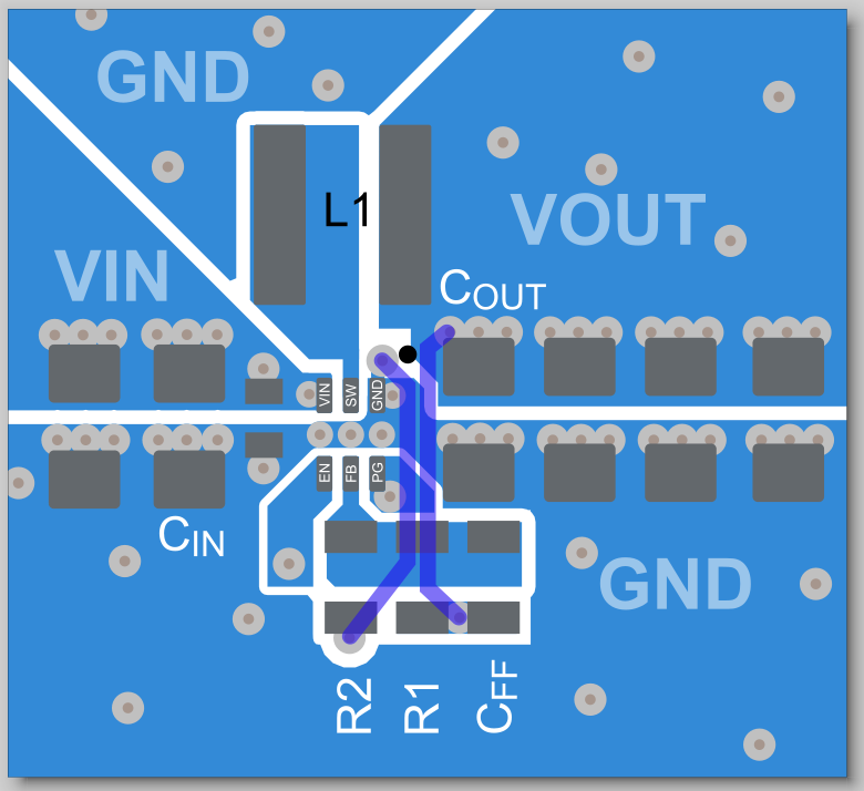
8.4.2
Layout Example
Figure 8-13
TPS62A04xB PCB Layout Recommendation