SLVSAM8D
July 2013 – August 2019
TPS63050
,
TPS63051
PRODUCTION DATA.
1
Features
2
Applications
3
Description
Device Images
Simplified Schematic (WCSP)
Efficiency vs Output Current
4
Revision History
5
Device Comparison Table
6
Pin Configuration and Functions
Pin Functions
7
Specifications
7.1
Absolute Maximum Ratings
7.2
ESD Ratings
7.3
Recommended Operating Conditions
7.4
Thermal Information
7.5
Electrical Characteristics
7.6
Switching Characteristics
7.7
Typical Characteristics
8
Detailed Description
8.1
Overview
8.2
Functional Block Diagrams
8.3
Feature Description
8.3.1
Power Good
8.3.2
Overvoltage Protection
8.3.3
Undervoltage Lockout (UVLO)
8.3.4
Thermal Shutdown
8.3.5
Soft Start
8.3.6
Short Circuit Protection
8.4
Device Functional Modes
8.4.1
Control Loop Description
8.4.2
Power Save Mode Operation
8.4.3
Adjustable Current Limit
8.4.4
Device Enable
9
Application and Implementation
9.1
Application Information
9.2
Typical Application
9.2.1
Design Requirements
9.2.2
Detailed Design Procedure
9.2.2.1
Custom Design With WEBENCH® Tools
9.2.2.2
Output Filter Design
9.2.2.3
Inductor Selection
9.2.2.4
Capacitor selection
9.2.2.4.1
Input Capacitor
9.2.2.4.2
Output Capacitor
9.2.2.5
Setting the Output Voltage
9.2.3
Application Curves
10
Power Supply Recommendations
11
Layout
11.1
Layout Guidelines
11.2
Layout Example (WCSP)
11.3
Layout Example (HotRod)
11.4
Thermal Considerations
12
Device and Documentation Support
12.1
Custom Design With WEBENCH® Tools
12.2
Device Support
12.2.1
Third-Party Products Disclaimer
12.3
Related Links
12.4
Receiving Notification of Documentation Updates
12.5
Community Resources
12.6
Trademarks
12.7
Electrostatic Discharge Caution
12.8
Glossary
13
Mechanical, Packaging, and Orderable Information
Package Options
Mechanical Data (Package|Pins)
RMW|12
MPQF422
YFF|12
MXBG343
Thermal pad, mechanical data (Package|Pins)
Orderable Information
slvsam8d_oa
slvsam8d_pm
7.7
Typical Characteristics
V
OUT
= 3.3 V
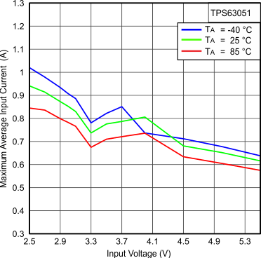
Figure 1.
Maximum Average Input Current vs Input Voltage
Figure 3.
Programmable Average Input Current vs Input Voltage
(1)
V
OUT
= 3.3 V
Figure 2.
Minimum Average Input Current vs Input Voltage
(1)
All options only available with the DSBGA package. For VQFN package ILIM1 is internally connected to voltage level > V
IH