SLVSGO6A december 2022 – august 2023 TPS631010 , TPS631011
PRODUCTION DATA
- 1
- 1 Features
- 2 Applications
- 3 Description
- 4 Revision History
- 5 Device Comparison Table
- 6 Pin Configuration and Functions
- 7 Specifications
-
8 Detailed Description
- 8.1 Overview
- 8.2 Functional Block Diagram
- 8.3 Feature Description
- 8.4 Device Functional Modes
- 9 Application and Implementation
- 10Device and Documentation Support
- 11Mechanical, Packaging, and Orderable Information
Package Options
Mechanical Data (Package|Pins)
- YBG|8
Thermal pad, mechanical data (Package|Pins)
Orderable Information
3 Description
The TPS631010 and TPS631011 are constant frequency peak current mode control buck-boost converters in tiny wafer chip scale package. They have a 3-A peak current limit (typical) and 1.6-V to 5.5-V input voltage range, and provide a power supply solution for system pre-regulators and voltage stabilizers.
Depending on the input voltage, the TPS631010 and TPS631011 automatically operate in boost, buck, or in 3-cycle buck-boost mode when the input voltage is approximately equal to the output voltage. The transitions between modes happen at a defined duty cycle and avoid unwanted toggling within the modes to reduce output voltage ripple. 8-μA quiescent current and power save mode enable the highest efficiency for light to no-load conditions.
The devices offer a very small solution size in WCSP.
| Part Number | Package(1) | Body Size (NOM) |
|---|---|---|
| TPS631010 | WCSP | 1.803 mm × 0.905 mm |
| TPS631011 |
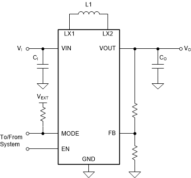
 Typical Application
 Efficiency vs Output Current (VOUT
= 3.3 V)