SLVS517B August 2004 – September 2015 TPS65013
PRODUCTION DATA.
- 1 Features
- 2 Applications
- 3 Description
- 4 Revision History
- 5 Pin Configuration and Functions
- 6 Specifications
-
7 Detailed Description
- 7.1 Overview
- 7.2 Functional Block Diagram
- 7.3
Feature Description
- 7.3.1
Battery Charger
- 7.3.1.1 Autonomous Power Source Selection
- 7.3.1.2 Temperature Qualification
- 7.3.1.3 Battery Preconditioning
- 7.3.1.4 Battery Charge Current
- 7.3.1.5 Battery Voltage Regulation
- 7.3.1.6 Charge Termination and Recharge
- 7.3.1.7 Sleep Mode
- 7.3.1.8 PG Output
- 7.3.1.9 Thermal Considerations for Setting Charge Current
- 7.3.2 Step-Down Converters, VMAIN and VCORE
- 7.3.3 Low-Dropout Voltage Regulators
- 7.3.4 Undervoltage Lockout
- 7.3.5 Power-Up Sequencing
- 7.3.6 System Reset and Control Signals
- 7.3.7 Vibrator Driver
- 7.3.1
Battery Charger
- 7.4 Device Functional Modes
- 7.5 Programming
- 7.6
Register Maps
- 7.6.1 CHGSTATUS Register (Address: 01h—Reset: 00h)
- 7.6.2 REGSTATUS Register (Address: 02h—Reset: 00h)
- 7.6.3 MASK1 Register (Address: 03h—Reset: FFh)
- 7.6.4 MASK2 Register (Address: 04h—Reset: FFh)
- 7.6.5 ACKINT1 Register (Address: 05h—Reset: 00h)
- 7.6.6 ACKINT2 Register (Address: 06h—Reset: 00h)
- 7.6.7 CHGCONFIG Register Address: 07h—Reset: 1Bh
- 7.6.8 LED1_ON Register (Address: 08h—Reset: 00h)
- 7.6.9 LED1_PER Register (Address: 09h—Reset: 00h)
- 7.6.10 LED2_ON Register (Address: 0Ah—Reset: 00h)
- 7.6.11 LED2_PER (Register Address: 0Bh—Reset: 00h)
- 7.6.12 VDCDC1 Register (Address: 0Ch—Reset: 32h/33h)
- 7.6.13 VDCDC2 Register (Address: 0Dh—Reset: 48h/78h)
- 7.6.14 VREGS1 Register (Address: 0Eh—Reset: 88h)
- 7.6.15 MASK3 Register (Address: 0Fh—Reset: 00h)
- 7.6.16 DEFGPIO Register Address: (10h—Reset: 00h)
- 8 Application and Implementation
- 9 Power Supply Recommendations
- 10Layout
- 11Device and Documentation Support
- 12Mechanical, Packaging, and Orderable Information
Package Options
Mechanical Data (Package|Pins)
- RGZ|48
Thermal pad, mechanical data (Package|Pins)
- RGZ|48
Orderable Information
6 Specifications
6.1 Absolute Maximum Ratings
over operating free-air temperature range unless otherwise noted(1)| MIN | MAX | UNIT | |
|---|---|---|---|
| Input voltage on VAC pin with respect to AGND | 20 | V | |
| Input voltage range on all other pins except AGND/PGND pins with respect to AGND | -0.3 | 7 | V |
| HBM and CDM capabilities at pins VIB, PG, and LED2 | 1 | kV | |
| Current at AC, VBAT, VINMAIN, L1, PGND1 | 1800 | mA | |
| Peak current at all other pins | 1000 | mA | |
| Continuous power dissipation | See Dissipation Ratings | ||
| Operating free-air temperature, TA | -40 | 85 | °C |
| Maximum junction temperature, TJ | 125 | °C | |
| Storage temperature range, Tstg | -65 | 150 | °C |
(1) Stresses beyond those listed under Absolute Maximum Ratings may cause permanent damage to the device. These are stress ratings only, and functional operation of the device at these or any other conditions beyond those indicated under Recommended Operating Conditions is not implied. Exposure to absolute-maximum-rated conditions for extended periods may affect device reliability.
6.2 ESD Ratings
| VALUE | UNIT | |||
|---|---|---|---|---|
| V(ESD) | Electrostatic discharge | Human body model (HBM), per ANSI/ESDA/JEDEC JS-001 (1) | 1000 | V |
| Charged device model (CDM), per JEDEC specification JESD22-C101(2) | 1000 | V | ||
(1) JEDEC document JEP155 states that 500-V HBM allows safe manufacturing with a standard ESD control process.
(2) JEDEC document JEP157 states that 250-V CDM allows safe manufacturing with a standard ESD control process.
6.3 Recommended Operating Conditions
| MIN | NOM | MAX | UNIT | ||
|---|---|---|---|---|---|
| V(AC) | Supply voltage from AC adapter | 4.5 | 5.5 | V | |
| V(USB) | Supply voltage from USB | 4.4 | 5.25 | V | |
| V(BAT) | Voltage at battery charger | 2.5 | 4.2 | V | |
| VI(MAIN),VI(CORE),VCC | Input voltage range step-down converters | 2.5 | 6.0 | V | |
| VI(LDO1), VI(LDO2) | Input voltage range for LDOs | 1.8 | 6.5 | V | |
| TA | Operating ambient temperature | -40 | 85 | °C | |
| TJ | Operating junction temperature | -40 | 125 | °C | |
| R(CC) | Resistor from VI(main),VI(core) to VCC used for filtering, CI(VCC) = 1 µF | 10 | 100 | Ω | |
6.4 Thermal Information
| THERMAL METRIC(1) | TPS65013 | UNIT | |
|---|---|---|---|
| RGZ (VQFN) | |||
| 48 PIN | |||
| RθJA | Junction-to-ambient thermal resistance | 27.0 | °C/W |
| RθJC(top) | Junction-to-case (top) thermal resistance | 14.3 | °C/W |
| RθJB | Junction-to-board thermal resistance | 4.6 | °C/W |
| ψJT | Junction-to-top characterization parameter | 0.2 | °C/W |
| ψJB | Junction-to-board characterization parameter | 4.6 | °C/W |
| RθJC(bot) | Junction-to-case (bottom) thermal resistance | 1.1 | °C/W |
(1) For more information about traditional and new thermal metrics, see the Semiconductor and IC Package Thermal Metrics application report, SPRA953.
6.5 Electrical Characteristics
VI(MAIN) = VI(CORE) = VCC = VI(LDO1) = VI(LDO2) = 3.6 V, TA = -40°C to 85°C, typical values are at TA = 25°C battery charger specifications are valid in the range 0°C < TA < 85°C unless otherwise noted| PARAMETER | TEST CONDITIONS | MIN | TYP | MAX | UNIT | ||
|---|---|---|---|---|---|---|---|
| CONTROL SIGNALS: LOW_PWR, SCLK, SDAT (INPUT) | |||||||
| VIH | High-level input voltage | IIH = 20 µA (1) | 1.2 | VCC | V | ||
| VIL | Low-level input voltage | IIL = 10 µA | 0 | 0.4 | V | ||
| IIB | Input bias current | 0.01 | 1.0 | µA | |||
| CONTROL SIGNALS: PB_ONOFF, HOT_RESET, BATT_COVER | |||||||
| VIH | High-level input voltage | IIH = 20 µA(1) | 0.8 VCC | 6 | V | ||
| VIL | Low-level input voltage | IIL = 10 µA | 0 | 0.4 | V | ||
| R(pb_onoff) | Pulldown resistor at PB_ONOFF | 1000 | kΩ | ||||
| R(hot_reset) | Pullup resistor at HOT_RESET, connected to VCC |
1000 | kΩ | ||||
| R(batt_cover) | Pulldown resistor at BATT_COVER | 2000 | kΩ | ||||
| t(glitch) | De-glitch time at all 3 pins | 38 | 56 | 77 | ms | ||
| t(batt_cover) | Delay after t(glitch) (PWRFAIL goes low) before supplies are disabled when BATT_COVER goes low. | 1.68 | 2.4 | 3.2 | ms | ||
| CONTROL SIGNALS: MPU_RESET, PWRFAIL, RESPWRON, INT, SDAT (OUTPUT) | |||||||
| VOH | High-level output voltage | 6 | V | ||||
| VOL | Low-level output voltage | IIL = 10 mA | 0 | 0.3 | V | ||
| td(mpu_nreset) | Duration of low pulse at MPU_RESET | 100 | µs | ||||
| td(nrespwron) | Duration of low pulse at RESPWRON after VMAIN is in regulation | TPOR = 0 | 80 | 100 | 120 | ms | |
| TPOR = 1 | 800 | 1000 | 1200 | ||||
| td(uvlo) | Time between UVLO going active (PWRFAIL going low) and supplies being disabled | 1.68 | 2.4 | 3.2 | ms | ||
| td(overtemp) | Time between chip overtemperature condition being recognized (PWRFAIL going low) and supplies being disabled | 1.68 | 2.4 | 3.2 | ms | ||
| SUPPLY PIN: VCC | |||||||
| I(Q) | Operating quiescent current | VI = 3.6 V, current into Main + Core + VCC | 70 | µA | |||
| IO(SD) | Shutdown supply current | VI = 3.6 V, BATT_COVER = GND, current into Main + Core + VCC |
15 | 25 | µA | ||
| VMAIN STEP-DOWN CONVERTER | |||||||
| VI | Input voltage range | 2.5 | 6.0 | V | |||
| IO | Maximum output current | 1000 | mA | ||||
| IO(SD) | Shutdown supply current | BATT_COVER = GND | 0.1 | 1 | µA | ||
| rDS(on) | P-channel MOSFET on-resistance | VI(MAIN) = VGS = 3.6 V | 110 | 210 | mΩ | ||
| Ilkg(p) | P-channel leakage current | V(DS) = 6 V | 1 | µA | |||
| rDS(on) | N-channel MOSFET on-resistance | VI(MAIN) = VGS = 3.6 V | 110 | 200 | mΩ | ||
| Ilkg(N) | N-channel leakage current | V(DS) = 6 V | 1 | µA | |||
| IL | P-channel current limit | 2.5 V < VI(MAIN) < 6 V | 1.4 | 1.75 | 2.1 | A | |
| fS | Oscillator frequency | 1 | 1.25 | 1.5 | MHz | ||
| VO(MAIN) | Fixed output voltage | 1.8 V | VI(MAIN) = 2.5 V to 6 V; IO= 0 mA | 0% | 3% | ||
| VI(MAIN) = 2.5 V to 6 V; 0 mA ≤ IO ≤ 1000 mA |
3% | 3% | |||||
| 2.75 V | VI(MAIN) = 2.95 V to 6 V; IO= 0 mA | 0% | 3% | ||||
| VI(MAIN) = 2.95 V to 6 V; 0 mA ≤ IO ≤ 1000 mA |
3% | 3% | |||||
| 3.0 V | VI(MAIN) = 3.2 V to 6 V; IO= 0 mA | 0% | 3% | ||||
| VI(MAIN) = 3.2 V to 6 V; 0 mA ≤ IO ≤ 1000 mA |
3% | 3% | |||||
| 3.3 V | VI(MAIN) = 3.5 V to 6 V; IO= 0 mA | 0% | 3% | ||||
| VI(MAIN) = 3.5 V to 6 V; 0 mA ≤ IO ≤ 1000 mA |
3% | 3% | |||||
| Line regulation | VI(MAIN) = VO(MAIN) + 0.5 V (min. 2.5 V) to 6 V, IO = 10 mA |
0.5 | %/V | ||||
| Load regulation | IO = 10 mA to 1000 mA | 0.12 | %/A | ||||
| R(VMAIN) | VMAIN discharge resistance | 400 | Ω | ||||
| VCORE STEP-DOWN CONVERTER | |||||||
| VI | Input voltage range | 2.5 | 6.0 | V | |||
| IO | Maximum output current | 400 | mA | ||||
| IO(SD) | Shutdown supply current | BATT_COVER = GND | 0.1 | 1 | µA | ||
| rDS(on) | P-channel MOSFET on-resistance | VI(CORE) = VGS = 3.6 V | 275 | 530 | mΩ | ||
| Ilkg(p) | P-channel leakage current | VDS = 6 V | 0.1 | 1 | µA | ||
| rDS(on) | N-channel MOSFET on-resistance | VI(CORE) = VGS = 3.6 V | 275 | 500 | mΩ | ||
| Ilkg(N) | N-channel leakage current | VDS = 6 V | 0.1 | 1 | µA | ||
| IL | P-channel current limit | 2.5 V < VI(CORE) < 6 V | 600 | 700 | 900 | mA | |
| fS | Oscillator frequency | 1 | 1.25 | 1.5 | MHz | ||
| VO(CORE) | Fixed output voltage | 0.85 V | VI(CORE) = 2.5 V to 6 V; IO= 0 mA, CO = 22 µF |
0% | 3% | ||
| VI(CORE) = 2.5 V to 6 V; 0 mA ≤ IO ≤ 400 mA, CO = 22 µF |
3% | 3% | |||||
| 1.05 V | VI(CORE) = 2.5 V to 6 V; IO = 0 mA, CO = 22 µF |
0% | 3% | ||||
| VI(CORE) = 2.5 V to 6 V; 0 mA ≤ IO ≤ 400 mA, CO = 22 µF |
3% | 3% | |||||
| 1.1 V | VI(CORE) = 2.5 V to 6 V; IO= 0 mA, CO = 22 µF |
0% | 3% | ||||
| VI(CORE) = 2.5 V to 6 V; 0 mA ≤ IO ≤ 400 mA, CO = 22 µF |
3% | 3% | |||||
| 1.2 V | VI(CORE) = 2.5 V to 6 V; IO = 0 mA | 0% | 3% | ||||
| VI(CORE) = 2.5 V to 6 V; 0 mA ≤ IO ≤ 400 mA | 3% | 3% | |||||
| 1.3 V | VI(CORE) = 2.5 V to 6 V; IO = 0 mA | 0% | 3% | ||||
| VI(CORE) = 2.5 V to 6 V; 0 mA ≤ IO ≤ 400 mA |
3% | 3% | |||||
| 1.4 V | VI(CORE) = 2.5 V to 6 V; IO = 0 mA | 0% | 3% | ||||
| VI(CORE) = 2.5 V to 6 V; 0 mA ≤ IO ≤ 400 mA |
3% | 3% | |||||
| 1.5 V | VI(CORE) = 2.5 V to 6 V; IO = 0 mA | 0% | 3% | ||||
| VI(CORE) = 2.5 V to 6 V; 0 mA ≤ IO ≤ 400 mA |
3% | 3% | |||||
| 1.6 V | VI(CORE) = 2.5 V to 6 V; IO = 0 mA | 0% | 3% | ||||
| VI(CORE) = 2.5 V to 6 V; 0 mA ≤ IO ≤ 400 mA |
3% | 3% | |||||
| Line regulation | VI(CORE) = VO(MAIN) + 0.5 V (min. 2.5 V) to 6 V, IO = 10 mA |
1 | %/V | ||||
| Load regulation | IO = 10 mA to 400 mA | 0.002 | %/mA | ||||
| R(VCORE) | VCORE discharge resistance | 400 | Ω | ||||
| VLDO1 AND VLDO2 LOW-DROPOUT REGULATORS | |||||||
| VI | Input voltage range | LD01 | 1.8 | 6.5 | V | ||
| LD02 | 1.8 | VCC | |||||
| VO | LDO1 output voltage range | 0.9 | VINLDO1 | V | |||
| Vref | Reference voltage | 485 | 500 | 515 | mV | ||
| VO | LDO2 output voltage range | 1.8 | 3.3 | V | |||
| IO | Maximum output current | Full-power mode | 200 | mA | |||
| Low-power mode | 30 | ||||||
| I(SC) | LDO1 & LDO2 short-circuit current limit | VLDO1 = GND, VLDO2 = GND | 650 | mA | |||
| Dropout voltage | IO = 200 mA, VINLDO1,2 = 1.8 V | 300 | mV | ||||
| Total accuracy | ±3% | ||||||
| Line regulation | VINLDO1,2 = VLDO1,2 + 0.5 V (min. 2.5 V) to 6.5 V, IO = 10 mA |
0.75 | %/V | ||||
| Load regulation | IO = 10 mA to 200 mA | 0.011 | %/mA | ||||
| Regulation time | Load change from 10% to 90% | 0.1 | ms | ||||
| Low-power mode | 0.1 | ||||||
| I(QFP) | LDO quiescent current (each LDO) | Full-power mode | 16 | 30 | µA | ||
| I(QLPM) | LDO quiescent current (each LDO) | Low-power mode | 12 | 18 | µA | ||
| IO(SD) | LDO shutdown current (each LDO) | 0.1 | 1 | µA | |||
| Ilkg(FB) | Leakage current feedback | 0.01 | 0.1 | µA | |||
(1) If the input voltage is higher than VCC, an additional input current, limited by an internal 10-kΩ resister, flows.
6.6 Battery Charger Electrical Characteristics
VO(REG) + V(DO-MAX) ≤ V(CHG) = V(AC) or V(USB), I(TERM) < IO ≤ 1 A, 0°C < TA < 85°C| PARAMETER | TEST CONDITIONS | MIN | TYP | MAX | UNIT | ||
|---|---|---|---|---|---|---|---|
| V(AC) | Input voltage range | 4.5 | 5.5 | V | |||
| V(USB) | Input voltage range | 4.35 | 5.25 | V | |||
| ICC(VCHG) | Supply current | V(CHG) > V(CHG)min | 1.2 | 2 | mA | ||
| ICC(SLP) | Sleep current | Sum of currents into VBAT pin, V(CHG) < V(SLP-ENTRY), 0°C ≤ TJ ≤ 85°C |
2 | 5 | µA | ||
| ICC(STBY) | Standby current | Current into USB pin | 45 | µA | |||
| Current into AC pin | 200 | 400 | |||||
| VOLTAGE REGULATOR | |||||||
| VO | Output voltage | V(CHG)min ≥ 4.5 V | 4.15 | 4.20 | 4.25 | V | |
| VDO | Dropout voltage (V(AC) - VBAT) | VO(REG) + V(DO-MAX) ≤ V(CHG), IO(OUT) = 1 A |
500 | 800 | mV | ||
| Dropout voltage (V(USB) - VBAT) | VO(REG) + V(DO-MAX) ≤ V(CHG), IO(OUT) = 0.5 A |
300 | 500 | mV | |||
| Dropout voltage (V(USB) - VBAT) | VO(REG) + V(DO-MAX) ≤ V(CHG), IO(OUT) = 0.1 A |
100 | 150 | mV | |||
| CURRENT REGULATION | |||||||
| IO(AC) | Output current range for AC operation(1) | VCHG ≥ 4.5 V, VI(OUT) > V(LOWV), V(AC) - VI(BAT) > V(DO-MAX) |
100 | 1000 | mA | ||
| V(SET) | Output current set voltage for AC operation at ISET pin. 100% output current I2C register CHGCONFIG<4:3> = 11 | Vmin ≥ 4.5 V, VI(BAT) > V(LOWV), V(AC) - VI(BAT) > V(DO-MAX) | 2.45 | 2.50 | 2.55 | V | |
| 75% output current I2C register CHGCONFIG<4:3> = 10 | 1.83 | 1.91 | 1.99 | V | |||
| 50% output current I2C register CHGCONFIG<4:3> = 01 | 1.23 | 1.31 | 1.39 | V | |||
| 32% output current I2C register CHGCONFIG<4:3> = 00 | 0.76 | 0.81 | 0.86 | V | |||
| KSET | Output current set factor for AC operation | 100 mA < IO < 1000 mA | 310 | 330 | 350 | ||
| 10 mA < IO < 100 mA | 300 | 340 | 380 | ||||
| IO(USB) | Output current range for USB operation | V(CHG)min ≥ 4.35 V, VI(BAT) > V(LOWV), V(USB) - VI(BAT) > V(DO-MAX),
I2C register CHGCONFIG<2> = 0 |
80 | 100 | mA | ||
| V(CHG)min ≥ 4.5 V, VI(BAT) > V(LOWV), VUSB - VI(BAT) > V(DO-MAX),
I2C register CHGCONFIG<2> = 1 |
400 | 500 | mA | ||||
| R(ISET) | Resistor range at ISET pin | 825 | 8250 | Ω | |||
| PRECHARGE CURRENT REGULATION, SHORT-CIRCUIT CURRENT, AND BATTERY DETECTION CURRENT | |||||||
| V(LOWV) | Precharge to fast-charge transition threshold, voltage on VBAT pin. |
V(CHG)min ≥ 4.5 V | 2.8 | 3.0 | 3.2 | V | |
| De-glitch time | V(CHG)min ≥ 4.5 V, VI(OUT) decreasing below threshold; 100-ns fall time, 10-mV overdrive | 8.8 | 23 | 60 | ms | ||
| I(PRECHG) | Precharge current (2) | 0 ≤ VI(OUT) < V(LOWV), t < t(PRECHG) | 10 | 100 | mA | ||
| I(DETECT) | Battery detection current | 200 | µA | ||||
| V(SET-PRECHG) | Voltage at ISET pin | 0 ≤ VI(OUT) < V(LOWV), t < t(PRECHG) | 240 | 255 | 270 | mV | |
| CHARGE TAPER AND TERMINATION DETECTION | |||||||
| I(TAPER) | Taper current detect range (3) | VI(OUT) > V(RCH), t < t(TAPER) | 10 | 100 | mA | ||
| V(SET_TAPER) | Voltage at ISET pin for charge TAPER detection | VI(OUT) > V(RCH), t < t(TAPER) | 235 | 250 | 265 | mV | |
| V(SET_TERM) | Voltage at ISET pin for charger termination detection(4) |
VI(OUT) > V(RCH) | 11 | 18 | 25 | mV | |
| De-glitch time for I(TAPER) | V(CHG)min ≥ 4.5 V, charging current increasing or decreasing above and below; 100-ns fall time, 10-mV overdrive |
8.8 | 23 | 60 | ms | ||
| De-glitch time for I(TERM) | V(CHG)min ≥ 4.5 V, charging current decreasing below;100-ns fall time, 10-mV overdrive | 8.8 | 23 | 60 | ms | ||
| TEMPERATURE COMPARATOR | |||||||
| V(LTF) | Low (cold) temperature threshold | 2.475 | 2.50 | 2.525 | V | ||
| V(HTF) | High (hot) temperature threshold | 0.485 | 0.5 | 0.515 | V | ||
| I(TS) | TS current source | 95 | 102 | 110 | µA | ||
| De-glitch time for temperature fault | 8.8 | 23 | 60 | ms | |||
| BATTERY RECHARGE THRESHOLD | |||||||
| V(RCH) | Recharge threshold | V(CHG)min≥ 4.5 V | VO(REG) -0.115 | VO(REG) -0.1 | VO(REG) -0.085 | V | |
| De-glitch time | V(CHG)min ≥ 4.5 V, VI(OUT) decreasing below threshold; 100-ns fall time, 10-mV overdrive |
8.8 | 23 | 60 | ms | ||
| TIMERS | |||||||
| t(PRECHG) | Precharge timer | V(CHG)min ≥ 4.5 V | 1500 | 1800 | 2160 | s | |
| t(TAPER) | Taper timer | V(CHG)min ≥ 4.5 V | 1500 | 1800 | 2160 | s | |
| t(CHG) | Charge timer | V(CHG)min ≥ 4.5 V | 15000 | 18000 | 21600 | s | |
| SLEEP AND STANDBY | |||||||
| V(SLP-ENTRY) | Sleep-mode entry threshold, PG output = high | 2.3 V ≤ VI(OUT) ≤ VO(REG) | V(CHG)≤ VI(OUT) +150 mV | V | |||
| V(SLP_EXIT) | Sleep-mode exit threshold,PG output = low | 2.3 V≤ VI(OUT) ≤ VO(REG) | V(CHG)≥ VI(OUT)+190 mV | V | |||
| De-glitch time for sleep mode entry and exit | AC or USB decreasing below threshold; 100-ns fall time, 10-mV overdrive | 8.8 | 23 | 60 | ms | ||
| t(USB_DEL) | Delay between valid USB voltage being applied and start of charging process from USB | 5 | ms | ||||
| CHARGER POWER-ON-RESET, UVLO, AND V(IN) RAMP RATE | |||||||
| V(CHGUVLO) | Charger undervoltage lockout | V(CHG) decreasing | 2.27 | 2.5 | 2.75 | V | |
| Hysteresis | 27 | mV | |||||
| V(CHGOVLO) | Charger overvoltage lockout | V(AC) increasing | 6.6 | V | |||
| Hysteresis | 0.5 | V | |||||
| CHARGER OVERTEMPERATURE SUSPEND | |||||||
| T(suspend) | Temperature at which charger suspends operation |
145 | °C | ||||
| T(hyst) | Hysteresis of suspend threshold | 20 | °C | ||||
| LOGIC SIGNALS DEFMAIN, DEFCORE, PS_SEQ, IFLSB | |||||||
| VIH | High-level input voltage | IIH = 20 µA | VCC-0.5 | VCC | V | ||
| VIL | Low-level input voltage | IIL = 10 µA | 0 | 0.4 | V | ||
| IIB | Input bias current | 0.01 | 1.0 | µA | |||
| LOGIC SIGNALS GPIO1-4 | |||||||
| VOL | Low-level output voltage | IOL = 1 mA, configured as an open-drain output |
0.3 | V | |||
| VOH | High-level output voltage | Configured as an open-drain output | 6 | V | |||
| VIL | Low-level input voltage | 0 | 0.4 | V | |||
| VIH | High-level input voltage | 1.2 | VCC (5) | V | |||
| II | Input leakage current | 1 | µA | ||||
| rDS(on) | Internal NMOS | VOL = 0.3 V | 150 | Ω | |||
| LOGIC SIGNALS PG, LED2 | |||||||
| VOL | Low-level output voltage | IOL = 20 mA | 0.5 | V | |||
| VOH | High-level output voltage | 6 | V | ||||
| VIBRATOR DRIVER VIB | |||||||
| VOL | Low-level output voltage | IOL = 100 mA | 0.3 | 0.5 | V | ||
| VOH | High-level output voltage | 6 | V | ||||
| THERMAL SHUTDOWN | |||||||
| T(SD) | Thermal shutdown | Increasing junction temperature | 160 | °C | |||
| UNDERVOLTAGE LOCKOUT | |||||||
| V(UVLO) | Undervoltage lockout threshold. The default value for UVLO is 2.75 V |
V(UVLO) 2.5 V | Filter resistor = 10R in series with VCC, VCC decreasing |
-3% | 3% | ||
| V(UVLO) 2.75 V | -3% | 3% | |||||
| V(UVLO) 3.0 V | -3% | 3% | |||||
| V(UVLO) 3.25 V | -3% | 3% | |||||
| V(UVLO_HYST) | UVLO comparator hysteresis | VCC rising | 350 | 400 | 450 | mV | |
| POWER GOOD | |||||||
| VMAIN, VCORE, VLDO1, VLDO2 decreasing |
-12% | -10% | -8% | ||||
| VMAIN, VCORE, VLDO1, VLDO2 increasing |
-7% | -5% | -3% | ||||
(1) 

(2) 

(3) 

(4) 

(5) If the input voltage is higher than VCC an additional current, limited by an internal 10-kΩ resistor, flows.
6.7 Serial Interface Timing Requirements
| MIN | MAX | UNIT | ||
|---|---|---|---|---|
| fMAX | Clock frequency | 400 | kHz | |
| twH(HIGH) | Clock high time | 600 | ns | |
| twL(LOW) | Clock low time | 1300 | ns | |
| tR | DATA and CLK rise time | 300 | ns | |
| tF | DATA and CLK fall time | 300 | ns | |
| th(STA) | Hold time (repeated) START condition (after this period the first clock pulse is generated) | 600 | ns | |
| th(DATA) | Setup time for repeated START condition | 600 | ns | |
| th(DATA) | Data input hold time | 0 | ns | |
| tsu(DATA) | Data input setup time | 100 | ns | |
| tsu(STO) | STOP condition setup time | 600 | ns | |
| t(BUF) | Bus free time | 1300 | ns | |
6.8 Dissipation Ratings
See (1)| AMBIENT TEMPERATURE |
MAX POWER DISSIPATION FOR TJ= 125°C(2) |
DERATING FACTOR ABOVE TA= 55°C |
|---|---|---|
| 25°C | 3 W | 30 mW/°C |
| 55°C | 2.1 W | 30 mW/°C |
(1) The TPS65013 is housed in a 48-pin QFN package with exposed leadframe on the underside. This 7 mm × 7 mm package exhibits a thermal impedance (junction-to-ambient) of 33 K/W when mounted on a JEDEC high-k board.
(2) Consideration needs to be given to the maximum charge current when the assembled application board exhibits a thermal impedance which differs significantly from the JEDEC high-k board.
6.9 Typical Characteristics
Table 1. Table of Graphs
| FIGURE | ||
|---|---|---|
| Efficiency | vs Output current | Figure 1, Figure 2, Figure 3, Figure 4 |
| Quiescent current | vs Input voltage | Figure 5 |
| Switching frequency | vs Temperature | Figure 6 |
| LDO1 Output voltage | vs Output current | Figure 7, Figure 8, Figure 9 |
| LDO2 Output voltage | vs Output current | Figure 10 |
| Line transient response (main) | Figure 11 | |
| Line transient response (core) | Figure 12 | |
| Line transient response (LDO1) | Figure 13 | |
| Line transient response (LDO2) | Figure 14 | |
| Load transient response (core) | Figure 15 | |
| Load transient response (main) | Figure 16 | |
| Load transient response (LDO1) | Figure 17 | |
| Load transient response (LDO2) | Figure 18 | |
| Output Ripple (PWM = 0) | Figure 19 | |
| Output Ripple (PWM = 1) | Figure 20 | |
| Start-up timing | Figure 21 | |
| Dropout voltage | vs Output current | Figure 22, Figure 23 |
| PSRR (LDO1 and LDO2) | vs Frequency | Figure 24 |
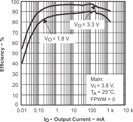 Figure 1. Efficiency vs Output Current
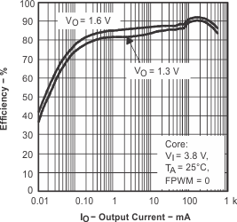 Figure 3. Efficiency vs Output Current
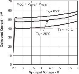 Figure 5. Quiescent Current vs Input Voltage
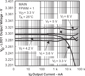 Figure 7. LD01 Output Voltage vs Output Current
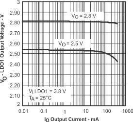 Figure 9. LDO1 Output Voltage vs Output Current
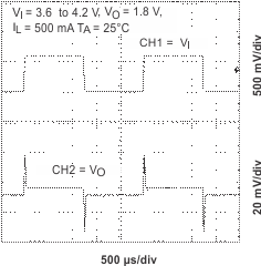 Figure 11. Line Transient Response (MAIN)
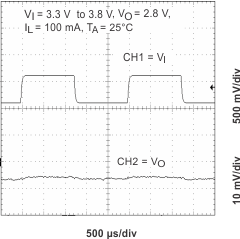 Figure 13. Line Transient Response (LDO1)
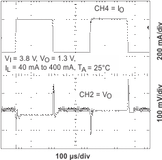 Figure 15. Load Transient Response (CORE)
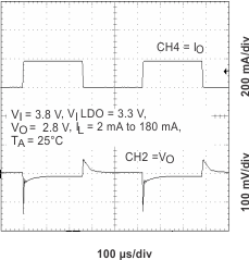 Figure 17. Load Transient Response (LDO1)
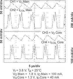 Figure 19. Output Ripple (PWM = 0)
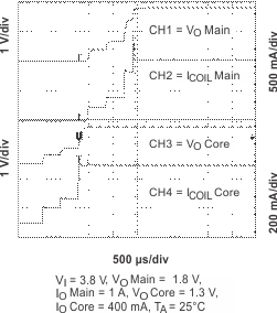 Figure 21. Start-Up Timing
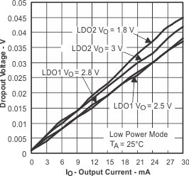 Figure 23. Dropout Voltage vs Output Current
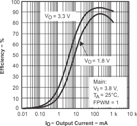 Figure 2. Efficiency vs Output Current
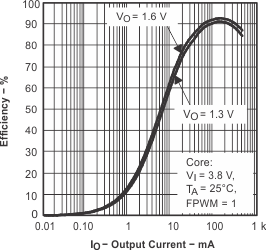 Figure 4. Efficiency vs Output Current
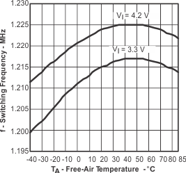 Figure 6. Switching Frequency vs Temperature
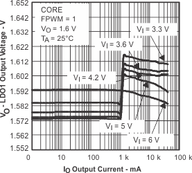 Figure 8. LD01 Output Voltage vs Output Current
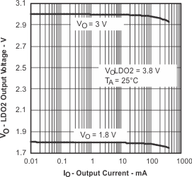 Figure 10. LDO2 Output Voltage vs Output Current
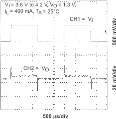 Figure 12. Line Transient Response (CORE)
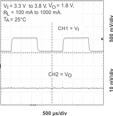 Figure 14. Line Transient Response (LDO2)
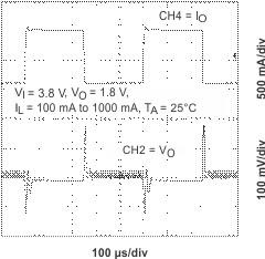 Figure 16. Load Transient Response (MAIN)
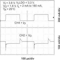 Figure 18. Load Transient Response (LDO2)
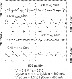 Figure 20. Output Ripple (PWM = 1)
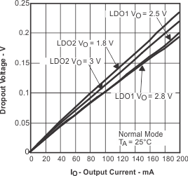 Figure 22. Dropout Voltage vs Output Current
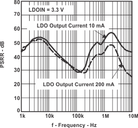 Figure 24. PSRR (LDO1, LDO2) vs Frequency