SLVS927F
March 2009 – July 2018
TPS65023-Q1
PRODUCTION DATA.
1
Features
2
Applications
3
Description
Device Images
Simplified Schematic
4
Revision History
5
Description (continued)
6
Pin Configuration and Functions
Pin Functions
7
Specifications
7.1
Absolute Maximum Ratings
7.2
ESD Ratings
7.3
Recommended Operating Conditions
7.4
Thermal Information
7.5
Electrical Characteristics
7.6
Timing Requirements
7.7
Typical Characteristics
8
Detailed Description
8.1
Overview
8.2
Functional Block Diagram
8.3
Feature Description
8.3.1
Step-Down Converters, VDCDC1, VDCDC2, and VDCDC3
8.3.2
Soft Start
8.3.3
Active Discharge When Disabled
8.3.4
Power-Good Monitoring
8.3.5
Low-Dropout Voltage Regulators
8.3.6
Undervoltage Lockout
8.4
Device Functional Modes
8.4.1
VRTC Output and Operation With or Without Backup Battery
8.4.2
Power-Save Mode Operation (PSM)
8.4.3
Low-Ripple Mode
8.4.4
100% Duty-Cycle Low-Dropout Operation
8.4.5
System Reset and Control Signals
8.4.5.1
DEFLDO1 and DEFLDO2
8.4.5.2
Interrupt Management and the INT Pin
8.5
Programming
8.5.1
Power-Up Sequencing
8.5.2
Serial Interface
8.6
Register Maps
8.6.1
VERSION Register (address: 00h) Read-Only
8.6.2
PGOODZ Register (address: 01h) Read-Only
Table 5.
PGOODZ Register Field Descriptions
8.6.3
MASK Register (address: 02h)
8.6.4
REG_CTRL Register (address: 03h)
Table 6.
REG_CTRL Register Field Descriptions
8.6.5
CON_CTRL Register (address: 04h)
Table 7.
CON_CTRL Register Field Descriptions
8.6.6
CON_CTRL2 Register (address: 05h)
Table 8.
CON_CTRL2 Register Field Descriptions
8.6.7
DEFCORE Register (address: 06h)
Table 9.
DEFCORE Register Field Descriptions
8.6.8
DEFSLEW Register (address: 07h)
Table 10.
DEFSLEW Register Field Descriptions
8.6.9
LDO_CTRL Register (address: 08h)
Table 11.
LDO_CTRL Register Field Descriptions
9
Application and Implementation
9.1
Application Information
9.1.1
Reset Condition of DCDC1
9.2
Typical Application
9.2.1
Design Requirements
9.2.2
Detailed Design Procedure
9.2.2.1
Inductor Selection for the DC-DC Converters
9.2.2.2
Output Capacitor Selection
9.2.2.3
Input Capacitor Selection
9.2.2.4
Output Voltage Selection
9.2.2.5
VRTC Output
9.2.2.6
LDO1 and LDO2
9.2.2.7
TRESPWRON
9.2.2.8
VCC Filter
9.2.3
Application Curves
10
Power Supply Recommendations
11
Layout
11.1
Layout Guidelines
11.2
Layout Example
12
Device and Documentation Support
12.1
Device Support
12.1.1
Third-Party Products Disclaimer
12.2
Documentation Support
12.2.1
Related Documentation
12.3
Receiving Notification of Documentation Updates
12.4
Community Resources
12.5
Trademarks
12.6
Electrostatic Discharge Caution
12.7
Glossary
13
Mechanical, Packaging, and Orderable Information
Package Options
Mechanical Data (Package|Pins)
RSB|40
MPQF185C
RHA|40
MPQF135D
Thermal pad, mechanical data (Package|Pins)
RSB|40
QFND094M
RHA|40
QFND047R
Orderable Information
slvs927f_oa
slvs927f_pm
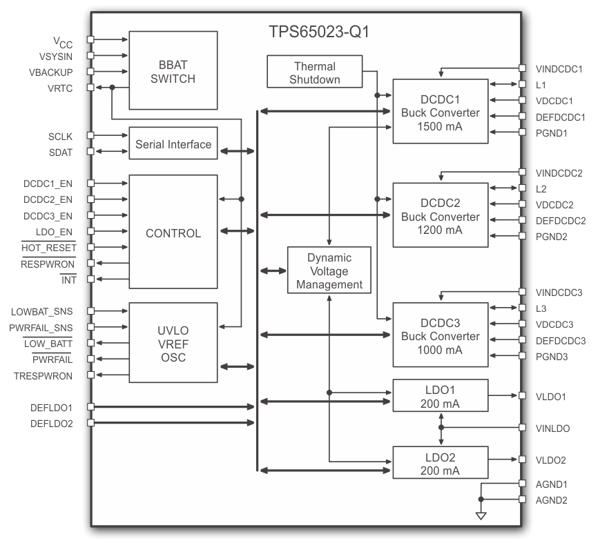
8.2
Functional Block Diagram