SLVS927F March   2009  – July 2018 TPS65023-Q1

PRODUCTION DATA.  

  1. Features
  2. Applications
  3. Description
    1.     Device Images
      1.      Simplified Schematic
  4. Revision History
  5. Description (continued)
  6. Pin Configuration and Functions
    1.     Pin Functions
  7. Specifications
    1. 7.1 Absolute Maximum Ratings
    2. 7.2 ESD Ratings
    3. 7.3 Recommended Operating Conditions
    4. 7.4 Thermal Information
    5. 7.5 Electrical Characteristics
    6. 7.6 Timing Requirements
    7. 7.7 Typical Characteristics
  8. Detailed Description
    1. 8.1 Overview
    2. 8.2 Functional Block Diagram
    3. 8.3 Feature Description
      1. 8.3.1 Step-Down Converters, VDCDC1, VDCDC2, and VDCDC3
      2. 8.3.2 Soft Start
      3. 8.3.3 Active Discharge When Disabled
      4. 8.3.4 Power-Good Monitoring
      5. 8.3.5 Low-Dropout Voltage Regulators
      6. 8.3.6 Undervoltage Lockout
    4. 8.4 Device Functional Modes
      1. 8.4.1 VRTC Output and Operation With or Without Backup Battery
      2. 8.4.2 Power-Save Mode Operation (PSM)
      3. 8.4.3 Low-Ripple Mode
      4. 8.4.4 100% Duty-Cycle Low-Dropout Operation
      5. 8.4.5 System Reset and Control Signals
        1. 8.4.5.1 DEFLDO1 and DEFLDO2
        2. 8.4.5.2 Interrupt Management and the INT Pin
    5. 8.5 Programming
      1. 8.5.1 Power-Up Sequencing
      2. 8.5.2 Serial Interface
    6. 8.6 Register Maps
      1. 8.6.1 VERSION Register (address: 00h) Read-Only
      2. 8.6.2 PGOODZ Register (address: 01h) Read-Only
        1. Table 5. PGOODZ Register Field Descriptions
      3. 8.6.3 MASK Register (address: 02h)
      4. 8.6.4 REG_CTRL Register (address: 03h)
        1. Table 6. REG_CTRL Register Field Descriptions
      5. 8.6.5 CON_CTRL Register (address: 04h)
        1. Table 7. CON_CTRL Register Field Descriptions
      6. 8.6.6 CON_CTRL2 Register (address: 05h)
        1. Table 8. CON_CTRL2 Register Field Descriptions
      7. 8.6.7 DEFCORE Register (address: 06h)
        1. Table 9. DEFCORE Register Field Descriptions
      8. 8.6.8 DEFSLEW Register (address: 07h)
        1. Table 10. DEFSLEW Register Field Descriptions
      9. 8.6.9 LDO_CTRL Register (address: 08h)
        1. Table 11. LDO_CTRL Register Field Descriptions
  9. Application and Implementation
    1. 9.1 Application Information
      1. 9.1.1 Reset Condition of DCDC1
    2. 9.2 Typical Application
      1. 9.2.1 Design Requirements
      2. 9.2.2 Detailed Design Procedure
        1. 9.2.2.1 Inductor Selection for the DC-DC Converters
        2. 9.2.2.2 Output Capacitor Selection
        3. 9.2.2.3 Input Capacitor Selection
        4. 9.2.2.4 Output Voltage Selection
        5. 9.2.2.5 VRTC Output
        6. 9.2.2.6 LDO1 and LDO2
        7. 9.2.2.7 TRESPWRON
        8. 9.2.2.8 VCC Filter
      3. 9.2.3 Application Curves
  10. 10Power Supply Recommendations
  11. 11Layout
    1. 11.1 Layout Guidelines
    2. 11.2 Layout Example
  12. 12Device and Documentation Support
    1. 12.1 Device Support
      1. 12.1.1 Third-Party Products Disclaimer
    2. 12.2 Documentation Support
      1. 12.2.1 Related Documentation
    3. 12.3 Receiving Notification of Documentation Updates
    4. 12.4 Community Resources
    5. 12.5 Trademarks
    6. 12.6 Electrostatic Discharge Caution
    7. 12.7 Glossary
  13. 13Mechanical, Packaging, and Orderable Information

Package Options

Mechanical Data (Package|Pins)
Thermal pad, mechanical data (Package|Pins)
Orderable Information

Output Voltage Selection

The DEFDCDC1, DEFDCDC2, and DEFDCDC3 pins are used to set the output voltage for each step-down converter. See Table 14 for the default voltages if the pins are pulled to GND or to VCC. If a different voltage is needed, an external resistor divider can be added to the DEFDCDCx pin as shown in Figure 47.

The output voltage of VDCDC1 is set with the I2C interface. If the voltage is changed from the default, using the DEFCORE register, the output voltage only depends on the register value. Any resistor divider at DEFDCDC1 does not change the voltage set with the register.

Table 14. DCDC1, DCDC2, and DCDC3 Default Voltage Levels

PIN LEVEL DEFAULT OUTPUT VOLTAGE
DEFDCDC1 VCC 1.6 V
GND 1.2 V
DEFDCDC2 VCC 3.3 V
GND 1.8 V
DEFDCDC3 VCC 3.3 V
GND 1.8 V

Using an external resistor divider at DEFDCDCx:
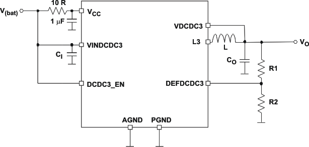
TPS65023-Q1 resist_divider_lvs927.gifFigure 47. External Resistor Divider

When a resistor divider is connected to DEFDCDCx, the output voltage can be set from 0.6 V up to the input voltage V(bat). The total resistance (R1 + R2) of the voltage divider should be kept in the 1-MR range to maintain a high efficiency at light load.

V(DEFDCDCx) = 0.6 V

Equation 8. TPS65023-Q1 q8_vout_lvs927.gif