SLVS927F March 2009 – July 2018 TPS65023-Q1
PRODUCTION DATA.
- 1 Features
- 2 Applications
- 3 Description
- 4 Revision History
- 5 Description (continued)
- 6 Pin Configuration and Functions
- 7 Specifications
-
8 Detailed Description
- 8.1 Overview
- 8.2 Functional Block Diagram
- 8.3 Feature Description
- 8.4 Device Functional Modes
- 8.5 Programming
- 8.6
Register Maps
- 8.6.1 VERSION Register (address: 00h) Read-Only
- 8.6.2 PGOODZ Register (address: 01h) Read-Only
- 8.6.3 MASK Register (address: 02h)
- 8.6.4 REG_CTRL Register (address: 03h)
- 8.6.5 CON_CTRL Register (address: 04h)
- 8.6.6 CON_CTRL2 Register (address: 05h)
- 8.6.7 DEFCORE Register (address: 06h)
- 8.6.8 DEFSLEW Register (address: 07h)
- 8.6.9 LDO_CTRL Register (address: 08h)
- 9 Application and Implementation
- 10Power Supply Recommendations
- 11Layout
- 12Device and Documentation Support
- 13Mechanical, Packaging, and Orderable Information
Package Options
Mechanical Data (Package|Pins)
Thermal pad, mechanical data (Package|Pins)
Orderable Information
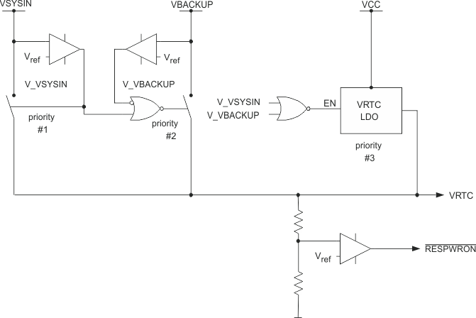
8.4.1 VRTC Output and Operation With or Without Backup Battery
The VRTC pin is an always-on output, intended to supply up to 30 mA to a permanently required rail (that is, for a real-time clock). The TPS65023-Q1 asserts the RESPWRON signal if VRTC drops below 2.4 V. VRTC is selected from a priority scheme based on the VSYSIN and VBACKUP inputs.
When the voltage at the VSYSIN pin exceeds 2.65 V, VRTC connects to the VSYSIN input through a PMOS switch and all other paths to VRTC are disabled. The PMOS switch drops a maximum of 375 mV at 30 mA, which should be considered when using VRTC. VSYSIN can be connected to any voltage source with the appropriate input voltage, including VCC or, if set to 3.3-V output, DCDC2 or DCDC3. When VSYSIN falls below 2.65 V or shorts to ground, the PMOS switch connecting VRTC and VSYSIN opens and VRTC then connects to either VBACKUP or the output of a dedicated 3-V, 30-mA LDO. TI recommends connecting VSYSIN to VCC or ground—VCC if a non-replaceable primary cell is connected to VBACKUP and ground if the VRTC output floats.
If the PMOS switch between VSYSIN and VRTC is open and VBACKUP exceeds 2.65 V, VRTC connects to VBACKUP through a PMOS switch. The PMOS switch drops a maximum of 375 mV at 30 mA, which should be considered if using VRTC. A typical application may connect VBACKUP to a primary Li button cell, but any battery that provides a voltage between 2.65 V and 6 V (that is, a single Li-Ion cell or a single boosted NiMH battery) is acceptable, to supply the VRTC output. In systems with no backup battery, the VBACKUP pin should be connected to GND.
If the switches between VRTC and VSYSIN or VBACKUP are open, the dedicated 3-V, 30-mA LDO, driven from VCC, connects to VRTC. This LDO is disabled if the voltage at the VSYSIN input exceeds 2.65 V.
Inside TPS65023-Q1 there is a switch (VMAX switch) which selects the higher voltage between VCC and VBACKUP. This is used as the supply voltage for some basic functions. The functions powered from the output of the VMAX switch are:
- INT output
- RESPWRON output
- HOT_RESET input
- LOW_BAT output
- PWRFAIL output
- Enable pins for DC-DC converters, LDO1 and LDO2
- Undervoltage lockout comparator (UVLO)
- Reference system with low-frequency timing oscillators
- LOW_BAT and PWRFAIL comparators
The main 2.25-MHz oscillator, and the I2C interface are only powered from VCC.
