SLVSBJ1B September 2012 – January 2017 TPS65051-Q1
PRODUCTION DATA.
- 1 Features
- 2 Applications
- 3 Description
- 4 Revision History
- 5 Pin Configuration and Functions
- 6 Specifications
-
7 Detailed Description
- 7.1 Overview
- 7.2 Functional Block Diagram
- 7.3
Feature Description
- 7.3.1 Operation
- 7.3.2 DCDC1 Converter
- 7.3.3 DCDC2 Converter
- 7.3.4 Dynamic Voltage Positioning
- 7.3.5 Soft Start
- 7.3.6 100% Duty-Cycle Low-Dropout Operation
- 7.3.7 Undervoltage Lockout
- 7.3.8 Mode Selection
- 7.3.9 Enable
- 7.3.10 RESET
- 7.3.11 Short-Circuit Protection
- 7.3.12 Thermal Shutdown
- 7.3.13 Low Dropout Voltage Regulators
- 7.4 Device Functional Modes
- 8 Application and Implementation
- 9 Power Supply Recommendations
- 10Layout
- 11Device and Documentation Support
- 12Mechanical, Packaging, and Orderable Information
Package Options
Mechanical Data (Package|Pins)
- RSM|32
Thermal pad, mechanical data (Package|Pins)
- RSM|32
Orderable Information
6 Specifications
6.1 Absolute Maximum Ratings
over operating free-air temperature range (unless otherwise noted)(1)| MIN | MAX | UNIT | ||
|---|---|---|---|---|
| VI | Input voltage on all pins except AGND, PGND, and EN_LDO1 pins with respect to AGND | –0.3 | 7 | V |
| Input voltage range on EN_LDO1 pins with respect to AGND | –0.3 | VCC + 0.5 | ||
| II | Current at VINDCDC1/2, L1, PGND1, L2, PGND2 | 1800 | mA | |
| Current at all other pins | 1000 | mA | ||
| VO | Output voltage for LDO1, LDO2, LDO3, and LDO4 | –0.3 | 4 | V |
| Continuous total power dissipation | See the Thermal Information | |||
| TA | Operating free-air temperature | –40 | 125 | °C |
| Tstg | Storage temperature | –65 | 150 | °C |
(1) Stresses beyond those listed under Absolute Maximum Ratings may cause permanent damage to the device. These are stress ratings only, which do not imply functional operation of the device at these or any other conditions beyond those indicated under Recommended Operating Conditions. Exposure to absolute-maximum-rated conditions for extended periods may affect device reliability.
6.2 ESD Ratings
| VALUE | UNIT | ||||
|---|---|---|---|---|---|
| V(ESD) | Electrostatic discharge | Human-body model (HBM), per AEC Q100-002(1) | 2000 | V | |
| Charged-device model (CDM), per AEC Q100-011 | 750 | V | |||
(1) AEC Q100-002 indicates that HBM stressing shall be in accordance with the ANSI/ESDA/JEDEC JS-001 specification.
6.3 Recommended Operating Conditions
over operating free-air temperature range (unless otherwise noted)| MIN | NOM | MAX | UNIT | ||
|---|---|---|---|---|---|
| VI | Input voltage for step-down converters, VINDCDC1/2 | 2.5 | 6 | V | |
| VO | Output voltage for step-down converter, VDCDC1 | 0.6 | VINDCDC1/2 | V | |
| Output voltage for step-down converter, VDCDC2 | 0.6 | VINDCDC1/2 | V | ||
| VI | Input voltage for LDOs, VINLDO1, VINLDO2, VINLDO3/4 | 1.5 | 6.5 | V | |
| VO | Output voltage for LDO1 and LDO2 | 1 | 3.6 | V | |
| Output voltage for LDO3 and LDO4 | 1 | 3.6 | V | ||
| IO | Output current at L1 (DCDC1) | 1000 | mA | ||
| Output current at L2 (DCDC2) | 600 | mA | |||
| Output current at VLDO1, VLDO2 | 400 | mA | |||
| Output current at VLDO3, VLDO4 | 200 | mA | |||
| Inductor at L1, L2(1) | 1.5 | 2.2 | μH | ||
| CO | Output capacitor at VDCDC1, VDCDC2(1) | 10 | 22 | μF | |
| Output capacitor at VLDO1, VLDO2, VLDO3, VLDO4(1) | 2.2 | μF | |||
| CI | Input capacitor at VCC(1) | 1 | μF | ||
| Input capacitor at VINLDO1, VINLDO2(1) | 2.2 | μF | |||
| Input capacitor at VINLDO3/4(1) | 2.2 | μF | |||
| TA | Operating ambient temperature | –40 | 125 | °C | |
| Resistor from battery voltage to VCC used for filtering(2) | 1 | 10 | Ω | ||
(1) See the Application Information section of this data sheet for more details.
(2) Up to 2 mA can flow into VCC; when both converters are running in PWM, this resistor causes the UVLO threshold to shift accordingly.
6.4 Thermal Information
| THERMAL METRIC(1) | TPS65051-Q1 | UNIT | |
|---|---|---|---|
| RSM (VQFN) | |||
| 32 PINS | |||
| RθJA | Junction-to-ambient thermal resistance | 37.2 | °C/W |
| RθJC(top) | Junction-to-case (top) thermal resistance | 30.1 | °C/W |
| RθJB | Junction-to-board thermal resistance | 7.8 | °C/W |
| ψJT | Junction-to-top characterization parameter | 0.4 | °C/W |
| ψJB | Junction-to-board characterization parameter | 7.6 | °C/W |
| RθJC(bot) | Junction-to-case (bottom) thermal resistance | 2.3 | °C/W |
(1) For more information about traditional and new thermal metrics, see the Semiconductor and IC Package Thermal Metrics application report.
6.5 Electrical Characteristics
VCC = VINDCDC1/2 = 3.6 V, EN = VCC, MODE = GND, L = 2.2 μH, CO = 10 μF, TA = –40°C to 125°C, typical values are at TA = 25°C (unless otherwise noted).| PARAMETER | TEST CONDITIONS | MIN | TYP | MAX | UNIT | ||
|---|---|---|---|---|---|---|---|
| SUPPLY CURRENT | |||||||
| VI | Input voltage range at VINDCDC1/2 | 2.5 | 6 | V | |||
| IQ | Operating quiescent current Total current into VCC, VINDCDC1/2, VINLDO1, VINLDO2, VINLDO3/4 |
One converter, IO = 0 mA. PFM mode enabled (Mode = GND) device not switching, EN_DCDC1 = VI OR EN_DCDC2 = VI; EN_LDO1= EN_LDO2 = EN_LDO3 = EN_LDO = GND |
20 | 30 | μA | ||
| Two converters, IO = 0 mA PFM mode enabled (Mode = 0) device not switching, EN_DCDC1 = VI AND EN_DCDC2 = VI; EN_LDO1 = EN_LDO2 = EN_LDO3 = EN_LDO4 = GND |
32 | 40 | μA | ||||
| One converter, IO = 0 mA. PFM mode enabled (Mode = GND) device not switching, EN_DCDC1 = VI OR EN_DCDC2 = VI; EN_LDO1 = EN_LDO2 = EN_LDO3 = EN_LDO4 = VI |
180 | 250 | μA | ||||
| IQ | Operating quiescent current into VCC | One converter, IO = 0 mA. Switching with no load (Mode = VI), PWM operation EN_DCDC1 = VI OR EN_DCDC2 = VI; EN_LDO1 = EN_LDO2 = EN_LDO3 = EN_LDO = GND |
0.85 | mA | |||
| Two converters, IO = 0 mA Switching with no load (Mode = VI), PWM operation EN_DCDC1 = VI AND EN_DCDC2 = VI; EN_LDO1 = EN_LDO2 = EN_LDO3 = EN_LDO = GND |
1.25 | mA | |||||
| I(SD) | Shutdown current | EN_DCDC1 = EN_DCDC2 = GND EN_LDO1 = EN_LDO2 = EN_LDO3 = EN_LDO4 = GND | 9 | 12 | μA | ||
| V(UVLO) | Undervoltage lockout threshold for DC-DC converters and LDOs | Voltage at VCC | 1.8 | 2 | V | ||
| EN_DCDC1, EN_DCDC2, DEFDCDC2, DEFLDO1, DEFLDO2, DEFLDO3, DEFLDO4, EN_LDO1, EN_LDO2, EN_LDO3, EN_LDO4 | |||||||
| VIH | High-level input voltage | MODE, EN_DCDC1, EN_DCDC2, DEFDCDC2, DEFLDO1, DEFLDO2, DEFLDO3, DEFLDO4, EN_LDO1, EN_LDO2, EN_LDO3, EN_LDO4 | 1.2 | VCC | V | ||
| VIL | Low-level input voltage | MODE, EN_DCDC1, EN_DCDC2, DEFLDO1, DEFLDO2, DEFLDO3, DEFLDO4, EN_LDO1, EN_LDO2, EN_LDO3, EN_LDO4, DEFDCDC2 | 0 | 0.4 | V | ||
| IlB | Input bias current | MODE = GND or VI MODE, EN_DCDC1, EN_DCDC2, DEFDCDC2, DEFLDO1, DEFLDO2, DEFLDO3, DEFLDO4, EN_LDO1, EN_LDO2, EN_LDO3, EN_LDO4 |
0.01 | 1 | μA | ||
| V_FB_LDOx = 1 V, FB_LDO1, FB_LDO2, FB_LDO3, FB_LDO4 | 100 | nA | |||||
| POWER SWITCH | |||||||
| rDS(on) | P-channel MOSFET on-resistance | DCDC1 | VINDCDC1/2 = 3.6 V | 280 | 630 | mΩ | |
| VINDCDC1/2 = 2.5 V | 400 | ||||||
| DCDC2 | VINDCDC1/2 = 3.6 V | 280 | 630 | ||||
| VINDCDC1/2 = 2.5 V | 400 | ||||||
| Ilkg | P-channel leakage current | VDCDCx = V(DS) = 6 V | 1 | μA | |||
| rDS(on) | N-channel MOSFET on-resistance | DCDC1 | VINDCDC1/2 = 3.6 V | 220 | 450 | mΩ | |
| VINDCDC1/2 = 2.5 V | 320 | ||||||
| DCDC2 | VINDCDC1/2 = 3.6 V | 220 | 450 | ||||
| VINDCDC1/2 = 2.5 V | 320 | ||||||
| Ilkg | N-channel leakage current | VDCDCx = V(DS) = 6 V | 7 | 10 | μA | ||
| I(LIMF) | Forward current limit PMOS (high side) and NMOS (low side) | DCDC1, 2.5 V ≤ VINDCDC1/2 ≤ 6 V | 1.19 | 1.4 | 1.65 | A | |
| DCDC2, 2.5 V ≤ VINDCDC1/2 ≤ 6 V | 0.85 | 1 | 1.15 | ||||
| Thermal shutdown | Increasing junction temperature | 150 | °C | ||||
| Thermal shutdown hysteresis | Decreasing junction temperature | 20 | °C | ||||
| OUTPUT | |||||||
| VO | Output-voltage range for DCDC1, DCDC2 | 0.6 | VINDCDC1/2 | V | |||
| Vref | Reference voltage | 600 | mV | ||||
| VO | DC output-voltage accuracy, DCDC1, DCDC2(1) | VINDCDC1/2 = 2.5 V to 6 V, 0 mA < IO = < IO(maximum) MODE = GND, PFM operation |
–2% | 0 | 2% | ||
| VINDCDC1/2 = 2.5 V to 6 V, 0 mA < IO = < IO(maximum) MODE = VI, PWM operation |
–1% | 0 | 1% | ||||
| ΔVO | Power-save-mode ripple voltage(2) | IO = 1 mA, MODE = GND, VO = 1.3 V, bandwith = 20 MHz | 25 | mVPP | |||
| VOL | RESET, PB_OUT output low voltage | IOL = 1 mA, Vhysteresis < 1 V, Vthreshold < 1 V | 0.2 | V | |||
| IOL | RESET, PB_OUT sink current | 1 | mA | ||||
| RESET, PB_OUT output leakage current | After PB_IN has been pulled high once; Vthreshold > 1 V and Vhysteresis > 1 V, VOH = 6 V | 10 | nA | ||||
| Vth | Vthreshold, Vhysteresis threshold | 0.98 | 1 | 1.02 | V | ||
| VLDO1, VLDO2, VLDO3 AND VLDO4 LOW-DROPOUT REGULATORS | |||||||
| VI | Input-voltage range for LDO1, LDO2, LDO3, LDO4 | 1.5 | 6.5 | V | |||
| V(FB) | Feedback voltage for FB_LDO1, FB_LDO2, FB_LDO3, and FB_LDO4 | 1 | V | ||||
| IO | Maximum output current for LDO1, LDO2 | 400 | mA | ||||
| Maximum output current for LDO3, LDO4 | 200 | ||||||
| I(SC) | LDO1 short-circuit current limit | VLDO1 = GND | 750 | mA | |||
| LDO2 short-circuit current limit | VLDO2 = GND | 850 | |||||
| LDO3 and LDO4 short-circuit current limit | VLDO3 = GND, VLDO4 = GND | 420 | |||||
| Dropout voltage at LDO1 | IO = 400 mA, VINLDO = 3.4 V | 400 | mV | ||||
| Dropout voltage at LDO2 | IO = 400 mA, VINLDO = 1.8 V | 280 | |||||
| Dropout voltage at LDO3, LDO4 | IO = 200 mA, VINLDO = 1.8 V | 280 | |||||
| Ilkg | Leakage current from VinLDOx to VLDOx | LDO enabled, VINLDO = 6.5 V, VO = 1 V at TA = 140°C | 3 | μA | |||
| VO | Output voltage accuracy for LDO1, LDO2, LDO3, LDO4 | IO = 10 mA | –2% | 1% | |||
| Line regulation for LDO1, LDO2, LDO3, LDO4 | VINLDO1,2 = VLDO1,2 + 0.5 V (minimum 2.5 V) to 6.5 V, VINLDO3,4 = VLDO3,4 + 0.5 V (minimum 2.5 V) to 6.5 V, IO = 10 mA |
–1% | 1% | ||||
| Load regulation for LDO1, LDO2, LDO3, LDO4 | IO = 0 mA to 400 mA for LDO1, LDO2 IO = 0 mA to 200 mA for LDO3, LDO4 |
–1% | 1% | ||||
| PSRR | Power-supply rejection ratio | f = 10 kHz; IO = 50 mA; VI = VO + 1 V | 70 | dB | |||
| R(DIS) | Internal discharge resistor at VLDO1, VLDO2, VLDO3, VLDO4 | Active when LDO is disabled | 350 | Ω | |||
| Thermal shutdown | Increasing junction temperature | 140 | °C | ||||
| Thermal shutdown hysteresis | Decreasing junction temperature | 20 | °C | ||||
(1) Output voltage specification does not include tolerance of external voltage-programming resistors.
(2) In power-save mode, device typically enters operation at IPSM = VI / 32 Ω.
6.6 Switching Characteristics
VCC = VINDCDC1/2 = 3.6 V, EN = VCC, MODE = GND, L = 2.2 μH, CO = 10 μF, TA = –40°C to 125°C, typical values are at TA = 25°C (unless otherwise noted).| PARAMETER | TEST CONDITIONS | MIN | TYP | MAX | UNIT | |
|---|---|---|---|---|---|---|
| OSCILLATOR | ||||||
| fSW | Oscillator frequency | 2.025 | 2.25 | 2.475 | MHz | |
| OUTPUT | ||||||
| tStart | Start-up time | Time from active EN to start switching | 170 | μs | ||
| tRamp | VOUT ramp-up time | Time to ramp from 5% to 95% of VO | 750 | μs | ||
| RESET delay time | Input voltage at threshold pin rising | 80 | 100 | 120 | ms | |
| PB-ONOFF debounce time | 26 | 32 | 38 | ms | ||
| VLDO1, VLDO2, VLDO3 AND VLDO4 LOW-DROPOUT REGULATORS | ||||||
| Regulation time for LDO1, LDO2, LDO3, LDO4 | Load change from 10% to 90% | 10 | μs | |||
6.7 Typical Characteristics
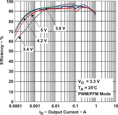 Figure 1. Efficiency vs Output Current
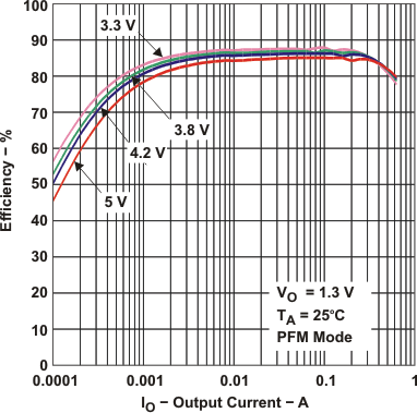 Figure 3. Efficiency vs Output Current
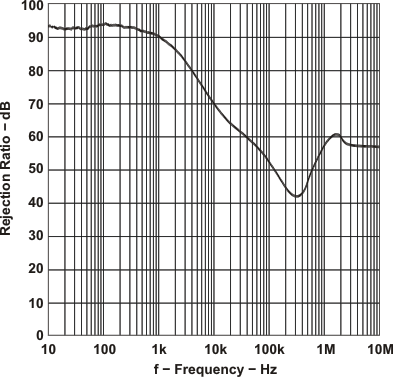 Figure 5. Power-Supply Rejection Ratio vs Frequency
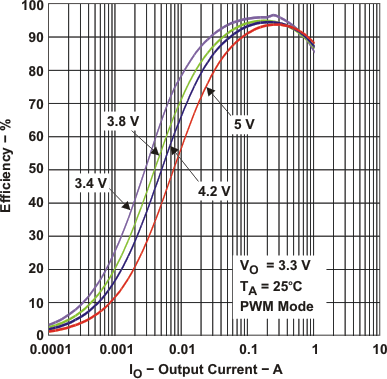 Figure 2. Efficiency vs Output Current
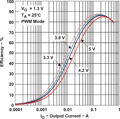 Figure 4. Efficiency vs Output Current