SWCS133E September 2015 – October 2024 TPS65094
PRODUCTION DATA
- 1
- 1 Features
- 2 Applications
- 3 Description
- 4 Device Options
- 5 Pin Configuration and Functions
-
6 Specifications
- 6.1 Absolute Maximum Ratings
- 6.2 ESD Ratings
- 6.3 Recommended Operating Conditions
- 6.4 Thermal Information
- 6.5 Electrical Characteristics: Total Current Consumption
- 6.6 Electrical Characteristics: Reference and Monitoring System
- 6.7 Electrical Characteristics: Buck Controllers
- 6.8 Electrical Characteristics: Synchronous Buck Converters
- 6.9 Electrical Characteristics: LDOs
- 6.10 Electrical Characteristics: Load Switches
- 6.11 Digital Signals: I2C Interface
- 6.12 Digital Input Signals (LDOLS_EN, SWA1_EN, THERMTRIPB, PMICEN, SLP_S3B, SLP_S4B, SLP_S0B)
- 6.13 Digital Output Signals (IRQB, RSMRSTB, PCH_PWROK, PROCHOT)
- 6.14 Timing Requirements
- 6.15 Switching Characteristics
- 6.16 Typical Characteristics
-
7 Detailed Description
- 7.1 Overview
- 7.2 Functional Block Diagram
- 7.3 Feature Description
- 7.4 Device Functional Modes
- 7.5 Programming
- 7.6
Register Maps
- 7.6.1 55
- 7.6.2 VENDORID: PMIC Vendor ID Register (offset = 00h) [reset = 0010 0010]
- 7.6.3 DEVICEID: PMIC Device and Revision ID Register (offset = 01h) [reset = OTP Dependent]
- 7.6.4 IRQ: PMIC Interrupt Register (offset = 02h) [reset = 0000 0000]
- 7.6.5 IRQ_MASK: PMIC Interrupt Mask Register (offset = 03h) [reset = 1111 1111]
- 7.6.6 PMICSTAT: PMIC Status Register (offset = 04h) [reset = 0000 0000]
- 7.6.7 OFFONSRC: PMIC Power Transition Event Register (offset = 05h) [reset = 0000 0000]
- 7.6.8 BUCK1CTRL: BUCK1 Control Register (offset = 20h) [reset = 0011 1000]
- 7.6.9 BUCK2CTRL: BUCK2 Control Register (offset = 21h) [reset = 0000 0000]
- 7.6.10 BUCK3CTRL: BUCK3 Control Register (offset = 23h) [reset = 0001 0001]
- 7.6.11 BUCK4CTRL: BUCK4 Control Register (offset = 25h) [reset = OTP Dependent]
- 7.6.12 BUCK5CTRL: BUCK5 Control Register (offset = 26h) [reset = OTP Dependent]
- 7.6.13 BUCK6CTRL: BUCK6 Control Register (offset = 27h) [reset = 0011 1101]
- 7.6.14 DISCHCNT1: Discharge Control1 Register (offset = 40h) [reset = 0101 0101]
- 7.6.15 DISCHCNT2: Discharge Control2 Register (offset = 41h) [reset = 0101 0101]
- 7.6.16 DISCHCNT3: Discharge Control3 Register (offset = 42h) [reset = 0000 0101]
- 7.6.17 POK_DELAY: PCH_PWROK Delay Register (offset = 43h) [reset = 0000 0111]
- 7.6.18 FORCESHUTDN: Force Emergency Shutdown Control Register (offset = 91h) [reset = 0000 0000]
- 7.6.19 BUCK4VID: BUCK4 VID Register (offset = 94h) [reset = 0010 1111]
- 7.6.20 BUCK5VID: BUCK5 VID Register (offset = 96h) [reset = 0100 1011]
- 7.6.21 BUCK6VID: BUCK6 VID Register (offset = 98h) [reset = OTP Dependent]
- 7.6.22 LDOA2VID: LDOA2 VID Register (offset = 9Ah) [reset = OTP Dependent]
- 7.6.23 LDOA3VID: LDOA3 VID Register (offset = 9Bh) [reset = OTP Dependent]
- 7.6.24 VR_CTRL1: BUCK1-3 Control Register (offset = 9Ch) [reset = OTP Dependent]
- 7.6.25 VR_CTRL2: VR Enable Register (offset = 9Eh) [reset = 0000 0000]
- 7.6.26 VR_CTRL3: VR Enable/Disable Register (offset = 9Fh) [reset = OTP Dependent]
- 7.6.27 GPO_CTRL: GPO Control Register (offset = A1h) [reset = 0010 0000]
- 7.6.28 PWR_FAULT_MASK1: VR Power Fault Mask1 Register (offset = A2h) [reset = 1100 0000]
- 7.6.29 PWR_FAULT_MASK2: VR Power Fault Mask2 Register (offset = A3h) [reset = 0011 0111]
- 7.6.30 DISCHCNT4: Discharge Control4 Register (offset = ADh) [reset = 0110 0001]
- 7.6.31 LDOA1CTRL: LDOA1 Control Register (offset = AEh) [reset = OTP Dependent]
- 7.6.32 PG_STATUS1: Power Good Status1 Register (offset = B0h) [reset = 0000 0000]
- 7.6.33 PG_STATUS2: Power Good Status2 Register (offset = B1h) [reset = 0000 0000]
- 7.6.34 TEMPHOT: Temperature Hot Status Register (offset = B5h) [reset = 0000 0000]
-
8 Application and Implementation
- 8.1 Typical Application
- 8.2 Specific Application for TPS650944
- 8.3 Dos and Don'ts
- Power Supply Recommendations
- 8.4 Layout
- 9 Device and Documentation Support
- 10Revision History
- 11Mechanical, Packaging, and Orderable Information
Package Options
Mechanical Data (Package|Pins)
- RSK|64
Thermal pad, mechanical data (Package|Pins)
- RSK|64
Orderable Information
8.2 Specific Application for TPS650944
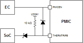
For the TPS650944 device, if register reset is desired when the PMICEN pin is pulled low, an alternate reset condition can be used. There are two simple options. The first option is to write 1 to the SDWN bit in the FORCESHUTDN register (see Section 7.6.18, FORCESHUTDN: Force Emergency Shutdown Control Register) to force power rails to turn off and reset all registers. The second option is to use the falling edge detection of the THERMTRIPB pin to trigger the device reset. In this case, when the PMICEN pin is pulled low, the THERMTRIPB pin on PMIC should be pulled low simultaneously, which can be done in several ways. One approach is to connect a low-voltage Schottky diode between the PMICEN and THERMTRIPB pins. Because the THERMTRIPB SoC pin is push-pull configured, a second diode is needed to prevent shorting the SoC pin to GND. An example can be seen in Figure 8-8. Both diodes must have a forward voltage below PMIC VIL (0.4 V) at the appropriate current. Another approach is to route the THERMTRIPB signal from SoC through the EC and tie PMICEN and THERMTRIPB together at the PMIC.

For the TPS650944 device, if both the PVINSWA1 and PVINSWB1_B2 pins are tied to 2.5 V, LDOA2 and LDOA3 will turn on if all VRs and load switches are enabled and have released their Power Good signals. To avoid LDOA2 and LDOA3 turning on unexpectedly, TI recommends using voltages other than 2.5 V on both SWA1 and SWB1_2.