SLVSC01A June   2013  – April 2015 TPS65133

PRODUCTION DATA.  

  1. Features
  2. Applications
  3. Description
  4. Typical Application
  5. Revision History
  6. Pin Configuration and Functions
  7. Specifications
    1. 7.1 Absolute Maximum Ratings
    2. 7.2 ESD Ratings
    3. 7.3 Recommended Operating Conditions
    4. 7.4 Thermal Information
    5. 7.5 Electrical Characteristics
    6. 7.6 Switching Characteristics
    7. 7.7 Typical Characteristics
  8. Detailed Description
    1. 8.1 Overview
    2. 8.2 Functional Block Diagram
    3. 8.3 Feature Description
      1. 8.3.1 Boost Converter (VPOS)
        1. 8.3.1.1 Switching Frequency (VPOS)
        2. 8.3.1.2 Output Voltage (VPOS)
        3. 8.3.1.3 Startup (VPOS)
        4. 8.3.1.4 Shutdown (VPOS)
        5. 8.3.1.5 Active Discharge (VPOS)
        6. 8.3.1.6 Short-Circuit Protection (VPOS)
      2. 8.3.2 Inverting Buck-Boost Converter (VNEG)
        1. 8.3.2.1 Switching Frequency (VNEG)
        2. 8.3.2.2 Output Voltage (VNEG)
        3. 8.3.2.3 Startup (VNEG)
        4. 8.3.2.4 Shutdown
        5. 8.3.2.5 Active Discharge (VNEG)
        6. 8.3.2.6 Short-Circuit Protection (VNEG)
      3. 8.3.3 Startup and Shutdown Sequencing
      4. 8.3.4 Thermal Shutdown
    4. 8.4 Device Functional Modes
      1. 8.4.1 Operation with VI < 2.9 V
      2. 8.4.2 Operation with VI ≈ VPOS (Diode Mode)
      3. 8.4.3 Operation with EN
  9. Application and Implementation
    1. 9.1 Application Information
    2. 9.2 Typical Application
      1. 9.2.1 Design Requirements
      2. 9.2.2 Detailed Design Procedure
        1. 9.2.2.1 Inductor Selection
        2. 9.2.2.2 Capacitor Selection
      3. 9.2.3 Application Performance Graphs
  10. 10Power Supply Recommendations
  11. 11Layout
    1. 11.1 Layout Guidelines
    2. 11.2 Layout Example
  12. 12Device and Documentation Support
    1. 12.1 Device Support
      1. 12.1.1 Third-Party Products Disclaimer
    2. 12.2 Community Resources
    3. 12.3 Trademarks
    4. 12.4 Electrostatic Discharge Caution
    5. 12.5 Glossary
  13. 13Mechanical, Packaging, and Orderable Information

Package Options

Mechanical Data (Package|Pins)
Thermal pad, mechanical data (Package|Pins)
Orderable Information

11 Layout

11.1 Layout Guidelines

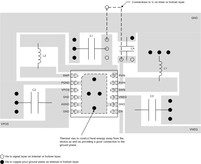
No PCB layout is perfect, and compromises are always necessary. However, the basic principles listed below (in order of importance) go a long way to achieving the full performance of the TPS65133 device.

  • Route discontinuous switching currents on the top layer using short, wide traces. Avoid routing these signals through vias, which have relatively high parasitic inductance and resistance.
  • Place C1 as close as possible to pin 12.
  • Place C2 as close as possible to pin 3. Place C3 as close as possible to pin 9.
  • Use the exposed thermal pad to connect GND, AGND and PGND.
  • Use a copper pour (preferably on layer 2) as a thermal spreader and connect it to the exposed thermal pad using a number of thermal vias.

Figure 28 illustrates how a PCB layout following the above principles may be realized in practice.
11.2 Layout Example

TPS65133 Layout_02_SLVSC01.gifFigure 28. PCB Layout Example