SLVSBC9C March 2012 – February 2016 TPS65177 , TPS65177A
PRODUCTION DATA.
- 1 Features
- 2 Applications
- 3 Description
- 4 Revision History
- 5 Pin Configuration and Functions
- 6 Specifications
-
7 Detailed Description
- 7.1 Overview
- 7.2 Functional Block Diagram
- 7.3 Feature Description
- 7.4
Device Functional Modes
- 7.4.1 Boost Converter (V(AVDD))
- 7.4.2 Buck 1 Converter (V(IO))
- 7.4.3 BUCK 2 CONVERTER (V(CORE))
- 7.4.4 Buck 3 Converter (V(HAVDD))
- 7.4.5 Positive Charge Pump Controller (V(GH)) with Temperature Compensation
- 7.4.6 Negative Charge Pump Controller (V(GL))
- 7.5 Gate Pulse Modulation (V(GHM))
- 7.6
Programming
- 7.6.1 I2C Serial Interface Description
- 7.6.2 Memory Description
- 7.6.3 Read / Write Description
- 7.6.4 Write Operation
- 7.6.5 READ OPERATION
- 7.6.6 Write Single Data to DAC:
- 7.6.7 Write Multiple Data to DAC (Auto Increment Address):
- 7.6.8 Write all DAC Data to EEPROM:
- 7.6.9 Read Single Data From DAC / EEPROM:
- 7.6.10 Read Multiple Data fFom DAC / EEPROM (Auto Increment Address):
- 7.7
Register Map
- 7.7.1
Registers and DAC Settings
- 7.7.1.1 Channel Register (with factory value) - 00h (00h)
- 7.7.1.2 Boost Output Voltage V(AVDD) Register (with factory value) - 01h (0Fh)
- 7.7.1.3 Boost HVS Offset Voltage Register (with factory value) - 02h (05h)
- 7.7.1.4 Boost Current Limit Negative Offset Current Register (with factory value) - 03h (00h)
- 7.7.1.5 Boost Soft-start Time Register (with factory value) - 04h (00h)
- 7.7.1.6 Buck 1 Output Voltage V(IO) Register (with factory value) - 05h (03h):
- 7.7.1.7 Buck 2 Output Voltage V(CORE) Register (with factory value) - 06h (02h)
- 7.7.1.8 Buck 3 Output Voltage V(HAVDD) Register (with factory value) - 07h (1Bh)
- 7.7.1.9 Pos. Charge Pump Low Output Voltage V(GH_L) Register (with factory value) - 08h (08h):
- 7.7.1.10 Positive Charge Pump Low Output Voltage V(GH_L) to V(GH_H) Positive Offset Voltage V(GH_OFS) Register (with factory value) - 09h (04h):
- 7.7.1.11 Gate Pulse Modulation Limit Voltage Register (with factory value) - 0Ah (00h)
- 7.7.1.12 Negative Charge Pump Output Voltage V(GL) Register (with factory value) - 0Bh (04h)
- 7.7.1.13 Buck 3 HVS Offset Voltage Register (with factory value) - 0Ch (00h):
- 7.7.1.14 Memory Write Remain Time Register (with factory value) - FEh (0Fh):
- 7.7.1
Registers and DAC Settings
- 8 Application and Implementation
- 9 Power Supply Recommendations
- 10Layout
- 11Device and Documentation Support
- 12Mechanical, Packaging, and Orderable Information
Package Options
Mechanical Data (Package|Pins)
- RHA|40
Thermal pad, mechanical data (Package|Pins)
Orderable Information
8 Application and Implementation
NOTE
Information in the following applications sections is not part of the TI component specification, and TI does not warrant its accuracy or completeness. TI’s customers are responsible for determining suitability of components for their purposes. Customers should validate and test their design implementation to confirm system functionality.
8.1 Application Information
Figure 19 shows a typical application circuit suitable for supplying LCD panels with GIP or non-GIP technology.
8.2 Typical Applications
 Figure 19. Typical Application
8.2.1 Design Requirements
For this design example, use the values shown in Table 6
Table 6. Design Parameters
| PARAMETER | VALUE |
|---|---|
| Voltage | VI = 12 V, V(AVDD) = 18 V, V(HAVDD) = 9 V, V(IO) = 3.3 V, V(CORE) = 1.2 V, V(GH) = 28 V, V(GL) = –10.3 V |
| Switching Frequency | Boost, Buck 1 = 750 kHz, Buck2, Buck 3 = 1 MHz |
8.2.2 Detailed Design Procedure
See the Device Functional Modes section for the detailed design procedure.
8.2.3 Application Curves
| PARAMETER | CONDITIONS | FIGURE |
|---|---|---|
| SEQUENCING | ||
| Power-on V(GL) driven by Buck 1 switch node | VI = 12 V, V(IO) = 3.3 V, V(CORE) = 1.2 V, V(AVDD) = 18 V, V(HAVDD) = 9 V, V(GH) = 28 V, V(GL) = –10.3 V |
Figure 20 |
| Power-on V(GL) driven by Boost switch node | VI = 12 V, V(IO) = 3.3 V, V(CORE) = 1.2 V, V(AVDD) = 18 V, V(HAVDD) = 9 V, V(GH) = 28 V, V(GL) = –10.3 V |
Figure 21 |
| Buck 1 Converter (VI = 12 V, L = 6.8 µH, COUT = 30 µF) | ||
| Efficiency vs. load current | V(IO) = 3.3 V | Figure 22 |
| PWM switching – light load | V(IO) = 3.3 V / 10 mA | Figure 23 |
| PWM switching – normal load | V(IO) = 3.3 V / 500 mA | Figure 24 |
| Load Transient response | V(IO) = 3.3 V / 100 mA → 500 mA | Figure 25 |
| Buck 2 Converter (VI = 3.3 V, L = 4.7 µH, COUT = 20 µF) | ||
| Efficiency vs. load current | V(CORE) = 1.2 V | Figure 26 |
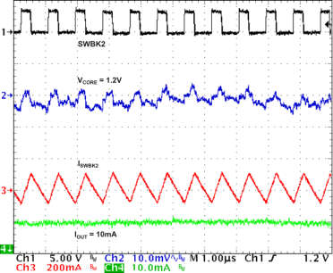
| PWM switching – light load | V(CORE) = 1.2 V / 10 mA | Figure 27 |
| PWM switching – normal load | V(CORE) = 1.2 V / 500 mA | Figure 28 |
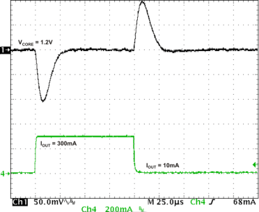
| Load Transient response | V(CORE) = 1.2 V / 10 mA → 300 mA | Figure 29 |
| Buck 3 Converter (VI = 12 V, L = 6.8 µH, COUT = 10 µF) | ||
| Efficiency vs. load current | V(HAVDD) = 9 V | Figure 30 |
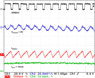
| PWM switching – light load sourcing | V(HAVDD) = 9 V / 10 mA | Figure 31 |
| PWM switching – light load sinking | V(HAVDD) = 9 V / -10 mA | Figure 32 |
| PWM switching –normal load sourcing | V(HAVDD) = 9 V / 500 mA | Figure 33 |
| PWM switching – normal load sinking | V(HAVDD) = 9 V / -500 mA | Figure 34 |
| Load Transient response | V(HAVDD) = 9 V / 0 mA → 300 mA → 0 mA → -350 mA | Figure 35 |
| Boost Converter (VI = 12 V, L = 6.8 µH, C(ISOSW) = 10 µF, COUT = 40 µF) | ||
| Efficiency vs. load current | V(AVDD) = 18 V | Figure 36 |
| PWM switching – light load | V(AVDD) = 18 V / 10 mA | Figure 37 |
| PWM switching – normal load | V(AVDD) = 18 V / 500 mA | Figure 38 |
| Load Transient response | V(AVDD) = 18 V / 100 mA → 500 mA | Figure 39 |
| Positive Charge-Pump (VI = 12 V, Diode = BAV99, R(SW) = 2.2 Ω, Transistor = KTA1666, COUT = 4.7 µF) | ||
| Light load operation | V(GH) = 28 V / 10 mA | Figure 40 |
| Normal load operation | V(GH) = 28 V / 50 mA | Figure 41 |
| Load Transient response | V(GH) = 28 V / 10 mA → 50 mA | Figure 42 |
| Negative Charge-Pump (VI = 12 V, Diode = BAV99, R(SW) = 2.2 Ω, Transistor = KTC4376, COUT = 4.7 µF) | ||
| Light load operation | V(GL) = –7.9 V / 10 mA | Figure 43 |
| Normal load operation | V(GL) = –7.9 V / 50 mA | Figure 44 |
| Load Transient response | V(GL) = –7.9 V / 10 mA → 50 mA | Figure 45 |
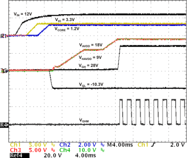
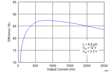
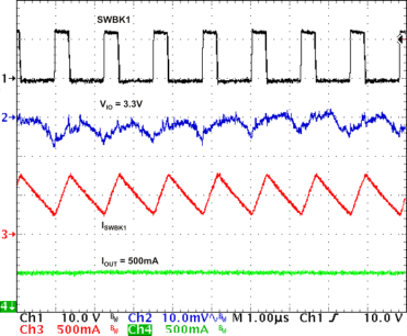

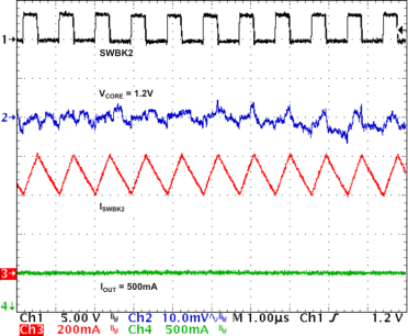
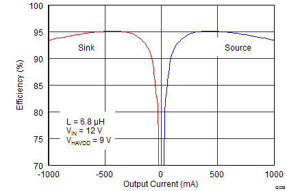

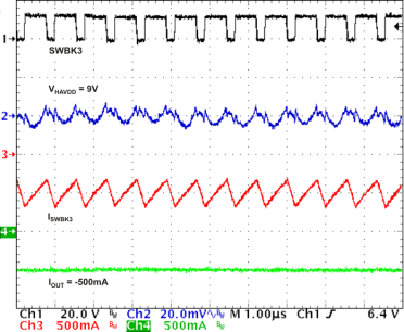
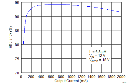
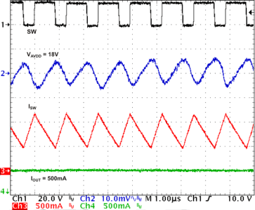


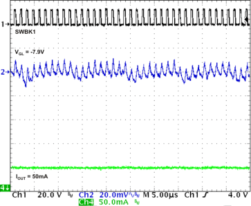

 Figure 23. Buck 1 (V(IO)) PWM Switching – Light Load



8.3 System Examples
 Figure 47. Gate Pulse Modulation Disabled (by I2C)
For best input voltage filtering low ESR ceramic capacitors are recommended. For better input voltage filtering the capacitor values can be increased.
- Internal logic: 100 nF close to the INVL-pin
- Boost converter: 10 µF near the inductor
- Buck 1 converter: 10 µF close to the INBK1-pins
- Buck 2 converter: 4.7 µF close to the INBK2-pin (also one of the Buck 2 output capacitors can be used)
- Buck 3 converter: 4.7 µF close to the INBK3-pin
Table 7. Input Capacitor Selection
| CAPACITOR | VOLTAGE RATING | TEMPERATURE CHARACTERISTICS | SUPPLIER(1) | COMPONENT CODE |
|---|---|---|---|---|
| 100 nF / 0402 | 16 V | X5R | Murata | GRM155R61C104KA88 |
| 100 nF / 0402 | 16 V | X5R | Taiyo Yuden | EMK105BJ104KV |
| 4.7 µF / 0402 | 6.3 V | X5R | Murata | GRM155R60J475ME87 |
| 4.7 µF / 0402 | 6.3 V | X5R | Taiyo Yuden | JMK105BBJ475MV |
| 4.7 µF / 0805 | 16 V | X5R | Murata | GRM21BR61C475KA88 |
| 4.7 µF / 0805 | 16 V | X5R | Taiyo Yuden | EMK212ABJ475KG |
| 10 µF / 1206 | 16 V | X5R | Murata | GRM31CR61C106KA88 |
| 10 µF / 1206 | 16 V | X7R | Taiyo Yuden | EMK316AB7106KL |
