SLVSBC9C March 2012 – February 2016 TPS65177 , TPS65177A
PRODUCTION DATA.
- 1 Features
- 2 Applications
- 3 Description
- 4 Revision History
- 5 Pin Configuration and Functions
- 6 Specifications
-
7 Detailed Description
- 7.1 Overview
- 7.2 Functional Block Diagram
- 7.3 Feature Description
- 7.4
Device Functional Modes
- 7.4.1 Boost Converter (V(AVDD))
- 7.4.2 Buck 1 Converter (V(IO))
- 7.4.3 BUCK 2 CONVERTER (V(CORE))
- 7.4.4 Buck 3 Converter (V(HAVDD))
- 7.4.5 Positive Charge Pump Controller (V(GH)) with Temperature Compensation
- 7.4.6 Negative Charge Pump Controller (V(GL))
- 7.5 Gate Pulse Modulation (V(GHM))
- 7.6
Programming
- 7.6.1 I2C Serial Interface Description
- 7.6.2 Memory Description
- 7.6.3 Read / Write Description
- 7.6.4 Write Operation
- 7.6.5 READ OPERATION
- 7.6.6 Write Single Data to DAC:
- 7.6.7 Write Multiple Data to DAC (Auto Increment Address):
- 7.6.8 Write all DAC Data to EEPROM:
- 7.6.9 Read Single Data From DAC / EEPROM:
- 7.6.10 Read Multiple Data fFom DAC / EEPROM (Auto Increment Address):
- 7.7
Register Map
- 7.7.1
Registers and DAC Settings
- 7.7.1.1 Channel Register (with factory value) - 00h (00h)
- 7.7.1.2 Boost Output Voltage V(AVDD) Register (with factory value) - 01h (0Fh)
- 7.7.1.3 Boost HVS Offset Voltage Register (with factory value) - 02h (05h)
- 7.7.1.4 Boost Current Limit Negative Offset Current Register (with factory value) - 03h (00h)
- 7.7.1.5 Boost Soft-start Time Register (with factory value) - 04h (00h)
- 7.7.1.6 Buck 1 Output Voltage V(IO) Register (with factory value) - 05h (03h):
- 7.7.1.7 Buck 2 Output Voltage V(CORE) Register (with factory value) - 06h (02h)
- 7.7.1.8 Buck 3 Output Voltage V(HAVDD) Register (with factory value) - 07h (1Bh)
- 7.7.1.9 Pos. Charge Pump Low Output Voltage V(GH_L) Register (with factory value) - 08h (08h):
- 7.7.1.10 Positive Charge Pump Low Output Voltage V(GH_L) to V(GH_H) Positive Offset Voltage V(GH_OFS) Register (with factory value) - 09h (04h):
- 7.7.1.11 Gate Pulse Modulation Limit Voltage Register (with factory value) - 0Ah (00h)
- 7.7.1.12 Negative Charge Pump Output Voltage V(GL) Register (with factory value) - 0Bh (04h)
- 7.7.1.13 Buck 3 HVS Offset Voltage Register (with factory value) - 0Ch (00h):
- 7.7.1.14 Memory Write Remain Time Register (with factory value) - FEh (0Fh):
- 7.7.1
Registers and DAC Settings
- 8 Application and Implementation
- 9 Power Supply Recommendations
- 10Layout
- 11Device and Documentation Support
- 12Mechanical, Packaging, and Orderable Information
Package Options
Mechanical Data (Package|Pins)
- RHA|40
Thermal pad, mechanical data (Package|Pins)
Orderable Information
6 Specifications
6.1 Absolute Maximum Ratings
over operating free-air temperature range (unless otherwise noted) (1)| VALUE | UNIT | |||
|---|---|---|---|---|
| MIN | MAX | |||
| Pin Voltage (2) | VIO, INBK1, HVS, INVL, INBK3, SWBK3, VHAVDD, SW, SWI, SWO | –0.3 | 20 | V |
| SWBK1 | –2 | 18 | V | |
| COMP, EN, A0, SDA, SCL, CTRL, SWBK2, VCORE, INBK2, DRVN, NTC | –0.3 | 7 | V | |
| VL | –0.3 | 5.5 | V | |
| DRVP, VGH, VGHM, RE | –0.3 | 40 | V | |
| VGL | –15 | 0.3 | V | |
| Operating junction temperature range | –40 | 150 | °C | |
| Storage temperature range, Tstg | –65 | 150 | °C | |
(1) Stresses beyond those listed under “absolute maximum ratings” may cause permanent damage to the device. These are stress ratings only and functional operation of the device at these or any other conditions beyond those indicated under “recommended operating conditions” is not implied. Exposure to absolute-maximum-rated conditions for extended periods may affect device reliability.
(2) With respect to the GND pin.
6.2 ESD Ratings
| VALUE | UNIT | |||
|---|---|---|---|---|
| V(ESD) | Electrostatic discharge | Human-body model (HBM), per ANSI/ESDA/JEDEC JS-001(1) | ±2000 | V |
| Charged-device model (CDM), per JEDEC specification JESD22-C101(2) | ±700 | |||
(1) JEDEC document JEP155 states that 500-V HBM allows safe manufacturing with a standard ESD control process.
(2) JEDEC document JEP157 states that 250-V CDM allows safe manufacturing with a standard ESD control process.
6.3 Recommended Operating Conditions
over operating free-air temperature range (unless otherwise noted)| MIN | TYP | MAX | UNIT | ||
|---|---|---|---|---|---|
| VI | Supply input voltage range | 8.6 | 12 | 14.7 | V |
| C(VL) | Internal 5 V regulator (VL) buffer capacitance (after DC-Bias derating) | 0.1 | 1 | 4.7 | µF |
| BOOST CONVERTER | |||||
| V(AVDD) | Boost output voltage range | 13.5 | 19.8 | V | |
| L | Boost inductor (inductor value that can be used) | 4.7 | 6.8 | 10 | µH |
| CI | Input capacitor placed at the inductor (ceramic capacitor value) | 4.7 | 10 | µF | |
| C(SWI) | Isolation Switch input capacitor (ceramic capacitor value) | 4.7 | 10 | 100 | µF |
| C(SWO) | Isolation Switch output capacitor (ceramic capacitor value) | 20 | 40 | 200 | µF |
| BUCK 1 CONVERTER | |||||
| V(IO) | Buck 1 output voltage range | 2.2 | 3.7 | V | |
| L | Buck 1 inductor (inductor value that can be used) | 4.7 | 6.8 | 10 | µH |
| CI | Buck 1 input capacitor (ceramic capacitor value) | 4.7 | 10 | µF | |
| COUT | Buck 1 output capacitor (ceramic capacitor value) | 20 | 30 | 100 | µF |
| BUCK 2 CONVERTER | |||||
| V(CORE) | Buck 2 output voltage range | 0.8 | 3.3 | V | |
| L | Buck 2 inductor (inductor value that can be used) | 4.7 | 6.8 | 10 | µH |
| CI | Buck 2 input capacitor (ceramic capacitor value) | 4.7 | 10 | µF | |
| COUT | Buck 2 output capacitor (ceramic capacitor value) | 10 | 20 | 50 | µF |
| BUCK 3 CONVERTER | |||||
| V(HAVDD) | Buck 3 output voltage range | 4.8 | 11.1 | V | |
| L | Buck 3 inductor (inductor value that can be used) | 4.7 | 6.8 | 10 | µH |
| CIN | Buck 3 input capacitor (ceramic capacitor value) | 4.7 | 10 | µF | |
| COUT | Buck 3 output capacitor (ceramic capacitor value) | 4.7 | 10 | 50 | µF |
| NEGATIVE CHARGE PUMP CONTROLLER | |||||
| V(GL) | Controller output voltage range | –5.5 | –14.5 | V | |
| C(FLY) | Flying capacitor (ceramic capacitor value) | 0.1 | 0.47 | 4.7 | µF |
| R(switch) | Resistance to the switch pin | 0 | 2.2 | 20 | Ω |
| COUT | Output capacitor (ceramic capacitor value) | 1 | 4.7 | 50 | µF |
| POSITIVE CHARGE PUMP CONTROLLER | |||||
| V(GH) | Controller output voltage range | 20 | 40 | V | |
| V(GH_offset) | Temperature compensation V(GH) positive offset | 0 | 15 | V | |
| C(FLY) | Flying capacitor (ceramic capacitor value) | 0.1 | 0.47 | 4.7 | µF |
| R(switch) | Resistance to the switch pin | 0 | 2.2 | 20 | Ω |
| COUT | Output capacitor (ceramic capacitor value) | 1 | 4.7 | 50 | µF |
| TEMPERATURE | |||||
| TA | Operating ambient temperature | –40 | 85 | °C | |
| TJ | Operating junction temperature | –40 | 125 | °C | |
6.4 Thermal Information
| THERMAL METRIC(1) | RHA (VQFN) | UNIT | |
|---|---|---|---|
| 40 PINS | |||
| RθJA | Junction-to-ambient thermal resistance | 32.8 | °C/W |
| RθJC(top) | Junction-to-case (top) thermal resistance | 20.3 | °C/W |
| RθJB | Junction-to-board thermal resistance | 7.9 | °C/W |
| ψJT | Junction-to-top characterization parameter | 0.3 | °C/W |
| ψJB | Junction-to-board characterization parameter | 7.8 | °C/W |
| RθJC(bot) | Junction-to-case (bottom) thermal resistance | 2.6 | °C/W |
(1) For more information about traditional and new thermal metrics, see the Semiconductor and IC Package Thermal Metrics application report, SPRA953.
6.5 Electrical Characteristics
VI = 12 V, EN = 3.3 V, V(AVDD) = 18 V, V(HAVDD) = 9 V, V(IO) = 3.3 V, V(CORE) = 1.2 V, V(GH) = 28 V, V(GL) = –10.3 V, TA = –40°C to 85°C, typical values are at TA = 25°C (unless otherwise noted)| PARAMETER | TEST CONDITIONS | MIN | TYP | MAX | UNIT | ||
|---|---|---|---|---|---|---|---|
| SUPPLY CURRENT | |||||||
| VI | Operating input voltage | 8.6 | 14.7 | V | |||
| VIT+ | Undervoltage lockout threshold (UVLO) | VI rising | 8 | 8.3 | 8.6 | V | |
| VIT– | Hysteresis VI falling | 0.75 | V | ||||
| Thermal shutdown | Junction temperature rising | 150 | ºC | ||||
| LOGIC SIGNALS | |||||||
| VIH | High-level input voltage | EN, HVS, SDA, SCL, A0, CTRL | 2 | V | |||
| VIL | Low-level input voltage | EN, HVS, A0, CTRL | 1 | V | |||
| SDA, SCL | 0.9 | V | |||||
| INTERNAL REGULATOR | |||||||
| V(VL) | Internal supply | 4.9 | 5 | 5.1 | V | ||
| ISOLATION SWITCH | |||||||
| rDS(ON) | MOSFET on-resistance | I(SWI) = 1 A | 100 | mΩ | |||
| BOOST CONVERTER (V(AVDD)) | |||||||
| Switching frequency | 600 | 750 | 900 | kHz | |||
| V(AVDD) | Output voltage range | 13.5 | 18 | 19 | V | ||
| Output voltage range for max. 500h | 19.8 | V | |||||
| High Voltage Stress Mode V(AVDD) positive offset | 0 | 3 | V | ||||
| Switch overvoltage protection | At SW pin, V(AVDD) rising | 20.5 | 22.5 | V | |||
| Output voltage tolerance | At TJ = 0 ºC to 85 ºC | 1% | |||||
| Feedback input bias current | 350 | 600 | µA | ||||
| rDS(on) | MOSFET on-resistance | I(SW) = current limit | 100 | 200 | mΩ | ||
| MOSFET current limit | At TJ = 0 ºC to 85 ºC | 4.25 | 5 | 5.75 | A | ||
| MOSFET current limit negative offset | 0 | 2.8 | A | ||||
| Line Regulation | 8.6 V ≤ VI ≤ 14.7 V, IOUT = 500 mA | 0.001 | %/V | ||||
| Load Regulation | 1 mA ≤ IOUT ≤ 2 A | 0.08 | %/A | ||||
| BUCK1 CONERTER (V(IO)) | |||||||
| Switching frequency | 600 | 750 | 900 | kHz | |||
| V(IO) | Output voltage range | 2.2 | 3.3 | 3.7 | V | ||
| Output voltage tolerance | At TJ = 0 ºC to 85ºC | 2% | |||||
| I | Feedback input bias current | 10 | 200 | µA | |||
| rDS(on) | MOSFET on-resistance | I(SWBK1) = current limit | 200 | 300 | mΩ | ||
| MOSFET current limit | At TJ = 0 ºC to 85 ºC | 2.8 | 3.5 | 4.2 | A | ||
| Line Regulation | 8.6 V ≤ VI ≤ 14.7 V, IOUT = 500 mA | 0.002 | %/V | ||||
| Load Regulation | 1 mA ≤ IOUT ≤ 2 A | 0.07 | %/A | ||||
| BUCK2 CONVERTER (V(CORE)) | |||||||
| Switching frequency | 0.5 | 1 | 2 | MHz | |||
| V(CORE) | Output voltage range | 0.8 | 1.2 | 3.3 | V | ||
| Output voltage tolerance | At TJ = 0 ºC to 85 ºC | 2% | |||||
| Feedback input bias current | 20 | 200 | µA | ||||
| rDS(on) | MOSFET on-resistance | I(SWBK2) = current limit | 175 | 300 | mΩ | ||
| MOSFET current limit | At TJ = 0 ºC to 85 ºC | 2.5 | 3 | 3.5 | A | ||
| Line Regulation | 2.2 V ≤ VI ≤ 3.7 V, IOUT = 500 mA | 0.001 | %/V | ||||
| Load Regulation | 1 mA ≤ IOUT ≤ 1.5 A | 0.2 | %/A | ||||
| BUCK3 CONVERTER (V(HAVDD)) | |||||||
| Switching frequency | 0.5 | 1 | 2 | MHz | |||
| V(HAVDD) | Output voltage range | 4.8 | 9 | 11.1 | V | ||
| Output Voltage Stress Mode V(HAVDD) positive offset | 0 | 1.5 | V | ||||
| Output voltage tolerance | At TJ = 0 ºC to 85 ºC | 1.5% | |||||
| Feedback input bias current | 90 | 200 | µA | ||||
| rDS(on) | MOSFET on-resistance | I(SWBK3) = current limit | 300 | 500 | mΩ | ||
| MOSFET current limit | At TJ = 0 ºC to 85 ºC | 1.2 | 1.5 | 1.8 | A | ||
| Line Regulation | 8.6 V ≤ VI ≤ 14.7 V, IOUT = 500 mA | 0.002 | %/V | ||||
| Load Regulation | 1 mA ≤ IOUT ≤ 1 A | 0.05 | %/A | ||||
| NEGATIVE CHARGE PUMP CONTROLLER (V(GL)) | |||||||
| V(GL) | Output voltage range | –5.5 | –10.3 | –14.5 | V | ||
| Output voltage tolerance | At TJ = 0 ºC to 85 ºC | 2.5% | |||||
| Feedback input bias current | 50 | 200 | µA | ||||
| I(DRVN) | Max. DRVN drive current | V(DRVN) = 0.6 V | 5 | 10 | mA | ||
| Resistor DRVN to GND | 50 | 100 | 200 | kΩ | |||
| Line Regulation | 8.6 V ≤ VI ≤ 14.7 V, IOUT = 50 mA | 0.015 | %/V | ||||
| Load Regulation | 1 mA ≤ IOUT ≤ 100 mA | 0.002 | %/mA | ||||
| POSITIVE CHARGE PUMP CONTROLLER (V(GH)) | |||||||
| V(GH) | Output voltage range | 20 | 28 | 35 | V | ||
| V(GH_offset) | Temp. compensation V(GH) positive offset | V(GH_offset) = 8 V | 0 | 8 | 15 | V | |
| Max. output voltage including V(GH_offset) | 40 | V | |||||
| Output voltage tolerance | At TJ = 0 ºC to 85 ºC | 2.5% | |||||
| Feedback input bias current | 120 | 200 | µA | ||||
| I(DRVP) | Max. DRVP drive current | V(DRVP) = 17 V | 5 | 10 | mA | ||
| Line Regulation | 8.6 V ≤ VI ≤ 14.7 V, IOUT = 50 mA | 0.001 | %/V | ||||
| Load Regulation | 1 mA ≤ IOUT ≤ 100 mA | 0.001 | %/mA | ||||
| GATE PULSE MODULATION (V(GHM)) | |||||||
| Gate Pulse Modulation falling limit | V(GHM) = 15 V | 0 | 5 | 15 | V | ||
| rDS(ON)M1 | VGH to VGHM on-resistance | CTRL = 3.3 V, I(VGHM) = 20 mA, V(GH) = 28 V |
3 | 5 | Ω | ||
| rDS(ON)M2 | VGHM to RE on-resistance | CTRL = GND, I(RE) = 20 mA, V(GHM) = 15 V | 3 | 5 | Ω | ||
| CTRL to VGHM propagation delay | CTRL rising | 150 | 250 | 360 | ns | ||
6.6 I2C Interface Timing Characteristics (1)
| PARAMETER | TEST CONDITIONS | MIN | TYP | MAX | UNIT | |
|---|---|---|---|---|---|---|
| fSCL | SCL clock frequency | Standard mode | 100 | kHz | ||
| Fast mode | 400 | kHz | ||||
| Fast mode plus | 1 | MHz | ||||
| tLOW | LOW period of the SCL clock | Standard mode | 4.7 | µs | ||
| Fast mode | 1.3 | µs | ||||
| tHIGH | HIGH period of the SCL clock | Standard mode | 4.0 | µs | ||
| Fast mode | 600 | ns | ||||
| tBUF | Bus free time between a STOP and START condition | Standard mode | 4.7 | µs | ||
| Fast mode | 1.3 | µs | ||||
| thd:STA | Hold time for a repeated START condition | Standard mode | 4.0 | µs | ||
| Fast mode | 600 | ns | ||||
| tsu:STA | Setup time for a repeated START condition | Standard mode | 4.7 | µs | ||
| Fast mode | 600 | ns | ||||
| tsu:STO | Setup time for STOP condition | Standard mode | 4.0 | µs | ||
| Fast mode | 600 | ns | ||||
| thd:DAT | Data hold time | Standard mode | 0 | 3.45 | µs | |
| Fast mode | 0 | 0.9 | µs | |||
| tsu:DAT | Data setup time | Standard mode | 250 | ns | ||
| Fast mode | 100 | ns | ||||
| CB | Capacitive load for SDA and SCL | 400 | pF | |||
| tRCL1 | Rise time of SCL signal after a repeated START condition and after an acknowledge bit | Standard mode | 20 + 0.1CB | 1000 | ns | |
| Fast mode | 20 + 0.1CB | 1000 | ns | |||
| tRCL | Rise time of SCL signal | Standard mode | 20 + 0.1CB | 1000 | ns | |
| Fast mode | 20 + 0.1CB | 300 | ns | |||
| tFCL | Fall time of SCL signal | Standard mode | 20 + 0.1CB | 300 | ns | |
| Fast mode | 20 + 0.1CB | 300 | ns | |||
| tRDA | Rise time of SDA signal | Standard mode | 20 + 0.1CB | 1000 | ns | |
| Fast mode | 20 + 0.1CB | 300 | ns | |||
| tFDA | Fall time of SDA signal | Standard mode | 20 + 0.1CB | 300 | ns | |
| Fast mode | 20 + 0.1CB | 300 | ns | |||
(1) Industry standard I2C timing characteristics. Not tested in production.
6.7 I2C Timing Diagram

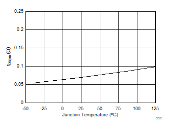
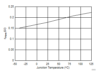
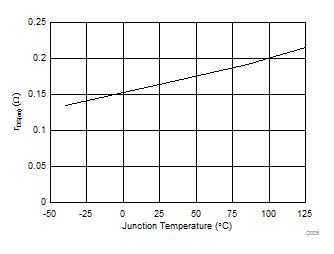
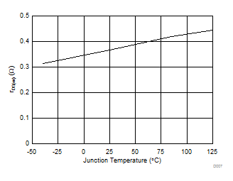
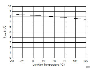
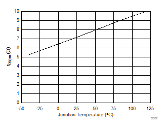
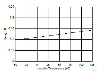
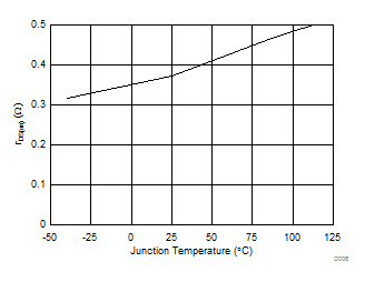
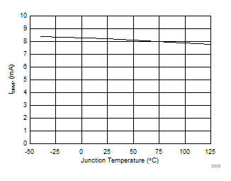
6.8 Typical Characteristics
VI = 12 V unless otherwise noted.