SLVSD80D November 2015 – May 2021 TPS65235
PRODUCTION DATA
- 1 Features
- 2 Applications
- 3 Description
- 4 Revision History
- 5 Pin Configuration and Functions
- 6 Specifications
-
7 Detailed Description
- 7.1 Overview
- 7.2 Functional Block Diagram
- 7.3
Feature Description
- 7.3.1 Boost Converter
- 7.3.2 Linear Regulator and Current Limit
- 7.3.3 Boost Converter Current Limit
- 7.3.4 Charge Pump
- 7.3.5 Slew Rate Control
- 7.3.6 Short Circuit Protection, Hiccup and Overtemperature Protection
- 7.3.7 Tone Generation
- 7.3.8 Tone Detection
- 7.3.9 Disable and Enable
- 7.3.10 Component Selection
- 7.4 Device Functional Modes
- 7.5 Programming
- 7.6 Register Maps
- 8 Application and Implementation
- 9 Power Supply Recommendations
- 10Layout
- 11Device and Documentation Support
- 12Mechanical, Packaging, and Orderable Information
Package Options
Mechanical Data (Package|Pins)
- RUK|20
Thermal pad, mechanical data (Package|Pins)
- RUK|20
Orderable Information
5 Pin Configuration and Functions
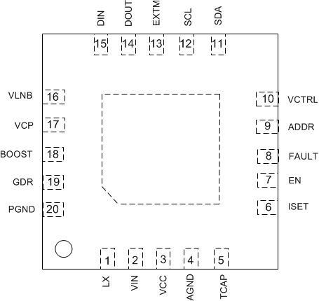
 Figure 5-1 20 Pin
(WQFN-20)RUK Package(Top View)
Figure 5-1 20 Pin
(WQFN-20)RUK Package(Top View)Table 5-1 Pin Functions
| PIN | I/O(1) | DESCRIPTION | |
|---|---|---|---|
| NAME | NO. | ||
| LX | 1 | I | Switching node of the boost converter |
| VIN | 2 | S | Input of internal linear regulator |
| VCC | 3 | O | Internal 6.3-V power supply. Connect a 1-μF ceramic capacitor from this pin to ground. When VIN is 5 V, connect VCC to VIN. |
| AGND | 4 | S | Analog ground. Connect all ground pins and power pad together. |
| TCAP | 5 | O | Connect a capacitor to this pin to set the rise time of the LNB output. |
| ISET | 6 | O | Connect a resistor to this pin to set the LNB output current limit. |
| EN | 7 | I | Enable pin to enable the VLNB output; pull to ground to disable output, and output will be pulled to ground, when the EN is low, the I2C can be accessed |
| FAULT | 8 | O | Oopen drain output pin, it goes low if any fault flag is set. |
| ADDR | 9 | I | Connecting different resistor to this pin to set different I2C address, see Table 7-4. |
| VCTRL | 10 | I | Voltage level at this pin to set the output voltage, see Table 7-3. |
| SDA | 11 | I/O | I2C compatible bi-directional data |
| SCL | 12 | I | I2C compatible clock input |
| EXTM | 13 | I | External modulation logic input pin which activates the 22-kHz tone output, feeding signal can be 22-kHz tone or logic high or low. |
| DOUT | 14 | O | Tone detection output |
| DIN | 15 | I | Tone detection input |
| VLNB | 16 | O | Output of the power supply connected to satellite receiver or switch. |
| VCP | 17 | O | Gate drive supply voltage, output of charge pump, connect a capacitor between this pin to pin VLNB. |
| BOOST | 18 | O | Output of the boost regulator and Input voltage of the internal linear regulator. |
| GDR | 19 | O | Control the gate of the external MOSFET for DiSEqc 2.x support. |
| PGND | 20 | S | Power ground for Boost Converter |
| Thermal PAD | Must be soldered to PCB for optimal thermal performance. Have thermal Vias on the PCB to enhance power dissipation. | ||
(1) I = input, O = output, I/O = input and output, S = power
supply