SLVSCW2A September 2015 – February 2016 TPS657095
PRODUCTION DATA.
- 1 Features
- 2 Applications
- 3 Description
- 4 Revision History
- 5 Pin Configuration and Functions
- 6 Specifications
-
7 Detailed Description
- 7.1 Overview
- 7.2 Functional Block Diagram
- 7.3
Feature Description
- 7.3.1 State Diagram
- 7.3.2 Power-up Timing
- 7.3.3 GPO
- 7.3.4 GPIO
- 7.3.5 LED_EN
- 7.3.6 PWM Dimming
- 7.3.7 Crystal Oscillator and CLKOUT
- 7.3.8 LDOs
- 7.3.9 Undervoltage Lockout
- 7.3.10 Power Up/Power Down Default States
- 7.3.11 Output Voltage Discharge for LDO1 and LDO2
- 7.3.12 Power-Good Status Bits for LDO1 and LDO2
- 7.3.13 Short-Circuit Protection
- 7.3.14 Thermal Shutdown
- 7.3.15 LED Driver
- 7.3.16 4kByte OTP Memory
- 7.4 Device Functional Modes
- 7.5 Programming
- 7.6
Register Map
- 7.6.1 DEV_AND_REV_ID Register Address: 00h
- 7.6.2 OTP_REV Register Address: 01h
- 7.6.3 GPIO_CTRL Register Address: 02h
- 7.6.4 PWM_OSC_CNTRL Register Address: 03h
- 7.6.5 ISINK_CURRENT Register Address: 04h
- 7.6.6 LDO_CTRL Register Address: 05h
- 7.6.7 LDO1_VCTRL Register Address: 06h
- 7.6.8 LDO2_VCTRL Register Address: 07h
- 7.6.9 PWM_DUTY_THR_L Register Address: 08h
- 7.6.10 PWM_DUTY_THR_H Register Address: 09h
- 7.6.11 RESERVED Register Address: 0Ah
- 7.6.12 PWM_DUTY_L Register Address: 0Bh
- 7.6.13 PWM_DUTY_H Register Address: 0Ch
- 7.6.14 RESERVED Register Address: 0Dh
- 7.6.15 SPARE Register Address: 0Eh
- 7.6.16 4K_OTP_PASSWORD Register Address: 0Fh
- 8 Application and Implementation
- 9 Power Supply Recommendations
- 10Layout
- 11Device and Documentation Support
- 12Mechanical, Packaging, and Orderable Information
Package Options
Mechanical Data (Package|Pins)
- YFF|16
Thermal pad, mechanical data (Package|Pins)
Orderable Information
10 Layout
10.1 Layout Guidelines
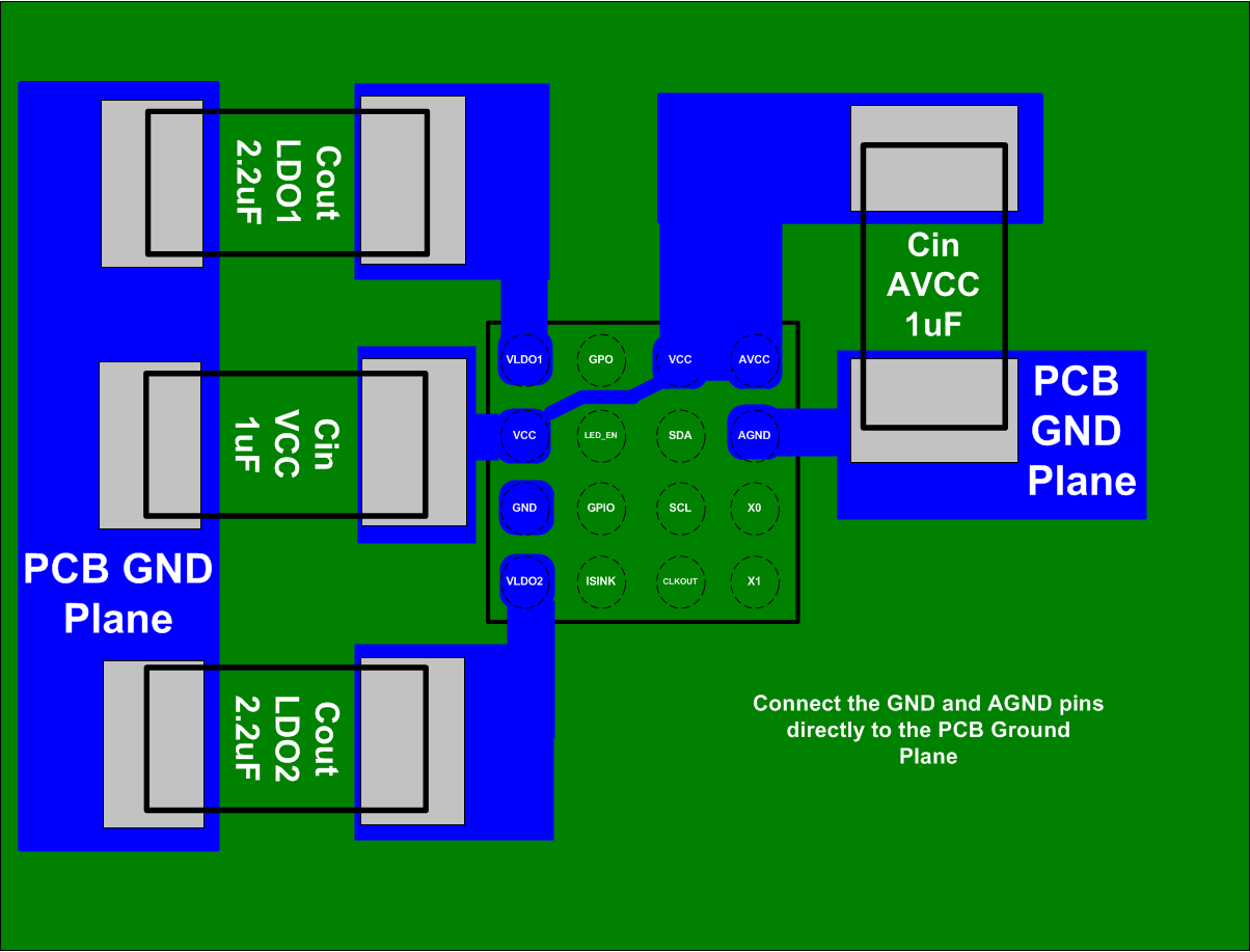
● The VCC and AVCC terminals should be bypassed to gorund with a low ESR ceramic bypass capacitor. The typical recommended bypass capacitance is 1uF with a X5R or X7R dielectric.
● The optimum placement is closest to the AVCC terminal and the AGND terminal.
● The AGND and GND terminals should be tied to the pcb ground plane at the terminal of the IC
10.2 Layout Example
