SLVSCW2A September 2015 – February 2016 TPS657095
PRODUCTION DATA.
- 1 Features
- 2 Applications
- 3 Description
- 4 Revision History
- 5 Pin Configuration and Functions
- 6 Specifications
-
7 Detailed Description
- 7.1 Overview
- 7.2 Functional Block Diagram
- 7.3
Feature Description
- 7.3.1 State Diagram
- 7.3.2 Power-up Timing
- 7.3.3 GPO
- 7.3.4 GPIO
- 7.3.5 LED_EN
- 7.3.6 PWM Dimming
- 7.3.7 Crystal Oscillator and CLKOUT
- 7.3.8 LDOs
- 7.3.9 Undervoltage Lockout
- 7.3.10 Power Up/Power Down Default States
- 7.3.11 Output Voltage Discharge for LDO1 and LDO2
- 7.3.12 Power-Good Status Bits for LDO1 and LDO2
- 7.3.13 Short-Circuit Protection
- 7.3.14 Thermal Shutdown
- 7.3.15 LED Driver
- 7.3.16 4kByte OTP Memory
- 7.4 Device Functional Modes
- 7.5 Programming
- 7.6
Register Map
- 7.6.1 DEV_AND_REV_ID Register Address: 00h
- 7.6.2 OTP_REV Register Address: 01h
- 7.6.3 GPIO_CTRL Register Address: 02h
- 7.6.4 PWM_OSC_CNTRL Register Address: 03h
- 7.6.5 ISINK_CURRENT Register Address: 04h
- 7.6.6 LDO_CTRL Register Address: 05h
- 7.6.7 LDO1_VCTRL Register Address: 06h
- 7.6.8 LDO2_VCTRL Register Address: 07h
- 7.6.9 PWM_DUTY_THR_L Register Address: 08h
- 7.6.10 PWM_DUTY_THR_H Register Address: 09h
- 7.6.11 RESERVED Register Address: 0Ah
- 7.6.12 PWM_DUTY_L Register Address: 0Bh
- 7.6.13 PWM_DUTY_H Register Address: 0Ch
- 7.6.14 RESERVED Register Address: 0Dh
- 7.6.15 SPARE Register Address: 0Eh
- 7.6.16 4K_OTP_PASSWORD Register Address: 0Fh
- 8 Application and Implementation
- 9 Power Supply Recommendations
- 10Layout
- 11Device and Documentation Support
- 12Mechanical, Packaging, and Orderable Information
Package Options
Mechanical Data (Package|Pins)
- YFF|16
Thermal pad, mechanical data (Package|Pins)
Orderable Information
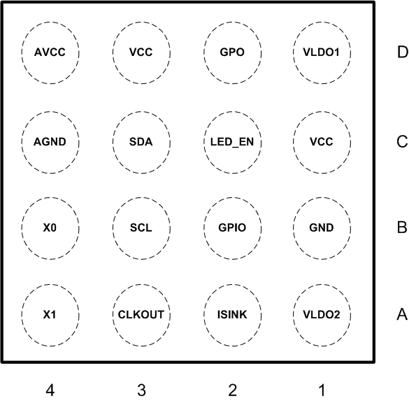
5 Pin Configuration and Functions
YFF Package
16-Pin DSBGA
Top View

Pin Functions
| PIN | I/O | DESCRIPTION | |
|---|---|---|---|
| NAME | NUMBER | ||
| VCC | C1, D3 | I | Supply Input. Connect a 1uF cap close to the C1 pin. Connect pins C1 and D3 together externally. |
| GND | B1 | I | Ground connection (main device ground - connect to ground plane on PCB) |
| AVCC | D4 | I | Analog Supply Input. Connect a 1uF cap close to pin. The D4 pin must be connected externally to the D3 and C1 pins. |
| AGND | C4 | I | Analog Ground connection (device quiet ground - connect to ground plane on PCB) |
| VLDO1 | D1 | O | Output voltage from LDO1 |
| VLDO2 | A1 | O | Output voltage from LDO2 |
| ISINK | A2 | O | Open drain current sink; connect to the cathode of LED |
| GPO | D2 | O | general purpose output |
| LED_EN | C2 | I | LED enable pin ( 0 = disabled, 1 = enabled) |
| GPIO | B2 | I | General Purpose Input/Output (see GPIO_CTRL Register for details) As an input, it is used to enable LDO2 |
| SCL | B3 | I | clock input for the I2C compatible interface |
| SDA | C3 | I/O | data input for the I2C compatible interface |
| XO | B4 | I | connection for external crystal to clock generator (input of amplifier) |
| XI | A4 | I | connection for external crystal to clock generator (output of amplifier) |
| CLKOUT | A3 | O | clock output |