SLVSE83B December 2020 – September 2023 TPS6593-Q1
PRODUCTION DATA
- 1
- 1 Features
- 2 Applications
- 3 Description
- 4 Revision History
- 5 Description (continued)
- 6 Pin Configuration and Functions
-
7 Specifications
- 7.1 Absolute Maximum Ratings
- 7.2 ESD Ratings
- 7.3 Recommended Operating Conditions
- 7.4 Thermal Information
- 7.5 General Purpose Low Drop-Out Regulators (LDO1, LDO2, LDO3)
- 7.6 Low Noise Low Drop-Out Regulator (LDO4)
- 7.7 Internal Low Drop-Out Regulators (LDOVRTC, LDOVINT)
- 7.8 BUCK1, BUCK2, BUCK3, BUCK4 and BUCK5 Regulators
- 7.9 Reference Generator (BandGap)
- 7.10 Monitoring Functions
- 7.11 Clocks, Oscillators, and PLL
- 7.12 Thermal Monitoring and Shutdown
- 7.13 System Control Thresholds
- 7.14 Current Consumption
- 7.15 Backup Battery Charger
- 7.16 Digital Input Signal Parameters
- 7.17 Digital Output Signal Parameters
- 7.18 I/O Pullup and Pulldown Resistance
- 7.19 I2C Interface
- 7.20 Serial Peripheral Interface (SPI)
- 7.21 Typical Characteristics
-
8 Detailed Description
- 8.1 Overview
- 8.2 Functional Block Diagram
- 8.3
Feature Description
- 8.3.1 System Supply Voltage Monitor
- 8.3.2
Power Resources (Bucks and LDOs)
- 8.3.2.1
Buck Regulators
- 8.3.2.1.1 BUCK Regulator Overview
- 8.3.2.1.2 Multi-Phase Operation and Phase-Adding or Shedding
- 8.3.2.1.3 Transition Between PWM and PFM Modes
- 8.3.2.1.4 Multi-Phase BUCK Regulator Configurations
- 8.3.2.1.5 Spread-Spectrum Mode
- 8.3.2.1.6 Adaptive Voltage Scaling (AVS) and Dynamic Voltage Scaling (DVS) Support
- 8.3.2.1.7 BUCK Output Voltage Setting
- 8.3.2.1.8 BUCK Regulator Current Limit
- 8.3.2.1.9 SW_Bx Short-to-Ground Detection
- 8.3.2.1.10 Sync Clock Functionality
- 49
- 8.3.2.2 Low Dropout Regulators (LDOs)
- 8.3.2.1
Buck Regulators
- 8.3.3 Output Voltage Monitor and PGOOD Generation
- 8.3.4 Thermal Monitoring
- 8.3.5 Backup Supply Power-Path
- 8.3.6 General-Purpose I/Os (GPIO Pins)
- 8.3.7 nINT, EN_DRV, and nRSTOUT Pins
- 8.3.8 Interrupts
- 8.3.9 RTC
- 8.3.10
Watchdog (WDOG)
- 8.3.10.1 Watchdog Fail Counter and Status
- 8.3.10.2 Watchdog Start-Up and Configuration
- 8.3.10.3 MCU to Watchdog Synchronization
- 8.3.10.4 Watchdog Disable Function
- 8.3.10.5 Watchdog Sequence
- 8.3.10.6 Watchdog Trigger Mode
- 8.3.10.7 WatchDog Flow Chart and Timing Diagrams in Trigger Mode
- 79
- 8.3.10.8 Watchdog Question-Answer Mode
- 8.3.11 Error Signal Monitor (ESM)
- 8.4
Device Functional Modes
- 8.4.1
Device State Machine
- 8.4.1.1 Fixed Device Power FSM
- 8.4.1.2
Pre-Configurable Mission States
- 8.4.1.2.1
PFSM Commands
- 8.4.1.2.1.1 REG_WRITE_IMM Command
- 8.4.1.2.1.2 REG_WRITE_MASK_IMM Command
- 8.4.1.2.1.3 REG_WRITE_MASK_PAGE0_IMM Command
- 8.4.1.2.1.4 REG_WRITE_BIT_PAGE0_IMM Command
- 8.4.1.2.1.5 REG_WRITE_WIN_PAGE0_IMM Command
- 8.4.1.2.1.6 REG_WRITE_VOUT_IMM Command
- 8.4.1.2.1.7 REG_WRITE_VCTRL_IMM Command
- 8.4.1.2.1.8 REG_WRITE_MASK_SREG Command
- 8.4.1.2.1.9 SREG_READ_REG Command
- 8.4.1.2.1.10 SREG_WRITE_IMM Command
- 8.4.1.2.1.11 WAIT Command
- 8.4.1.2.1.12 DELAY_IMM Command
- 8.4.1.2.1.13 DELAY_SREG Command
- 8.4.1.2.1.14 TRIG_SET Command
- 8.4.1.2.1.15 TRIG_MASK Command
- 8.4.1.2.1.16 END Command
- 8.4.1.2.2 Configuration Memory Organization and Sequence Execution
- 8.4.1.2.3 Mission State Configuration
- 8.4.1.2.4 Pre-Configured Hardware Transitions
- 8.4.1.2.1
PFSM Commands
- 8.4.1.3 Error Handling Operations
- 8.4.1.4 Device Start-up Timing
- 8.4.1.5 Power Sequences
- 8.4.1.6 First Supply Detection
- 8.4.1.7 Register Power Domains and Reset Levels
- 8.4.2 Multi-PMIC Synchronization
- 8.4.1
Device State Machine
- 8.5 Control Interfaces
- 8.6 Configurable Registers
- 8.7 Register Maps
- 9 Application and Implementation
- 10Device and Documentation Support
- 11Mechanical, Packaging, and Orderable Information
Package Options
Mechanical Data (Package|Pins)
- RWE|56
Thermal pad, mechanical data (Package|Pins)
- RWE|56
Orderable Information
8.3.2.2 Low Dropout Regulators (LDOs)
All of the LDO regulators in the TPS6593-Q1 device can be supplied by the system supply or another pre-regulated voltage source which are within the specified VIN range. The PVIN_LDOn voltage level must be equal or less than the VCCA voltage level to ensure proper operation of the LDOs. The default output voltages of all LDOs are loaded from the NVM memory and can be configured by the LDOn_VSET[7:0]. There is no hardware protection to prevent software from selecting an improper output voltage if the minimum level of PVIN_LDOn is lower than the dropout voltage of the LDO regulator in addition to the configured LDO output voltage. In such conditions, the output voltage droops to near the PVIN_LDOn level.
The LDO regulators do not have slew rate control for voltage ramp; by setting the LDOn_SLOW_RAMP bit to '1', however, the ramp up speed of the regulator output voltage is < 3 V/ms.
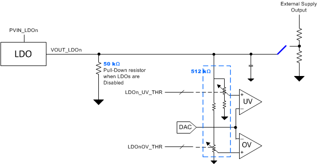
If an LDO is not needed, its associated UV/OV Voltage Monitor can be used to monitor an external voltage rail by connecting the external rail to the VOUT_LDOn pin. The voltage level of the monitored external rail must be within the PGOOD monitor range of the LDOn_VSET[7:0] of the LDO. If an external resistor divider is necessary in this case, the user must take into account the input impedance at the VOUT_LDOn pin (as shown in Figure 8-9), and adjust the resistor values to compensate for the voltage shift.
 Figure 8-9 Impedance at the
VOUT_LDOn Pins