SLVSER3A
November 2018 – April 2020
TPS65982BB
PRODUCTION DATA.
1
Features
2
Applications
3
Description
Device Images
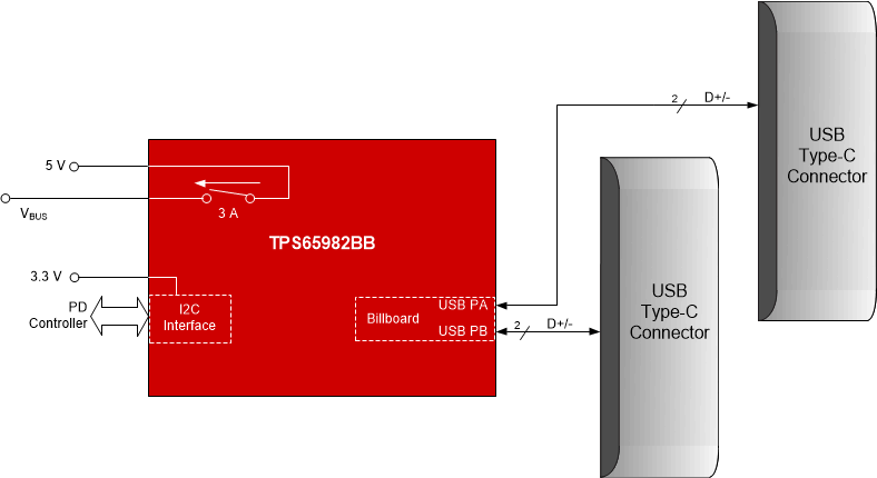
Simplified Diagram
4
Revision History
5
Pin Configuration and Functions
Pin Functions
6
Specifications
6.1
Absolute Maximum Ratings
6.2
ESD Ratings
6.3
Recommended Operating Conditions
6.4
Thermal Information
6.5
Power Supply Characteristics
6.6
Power Supervisor Characteristics
6.7
Power Consumption Characteristics
6.8
Port-Power Switch Characteristics
6.9
Port-Data Multiplexer Characteristics
6.10
Port-Data Multiplexer Clamp Characteristics
6.11
Port-Data Multiplexer Signal Monitoring Pullup and Pulldown Characteristics
6.12
USB Endpoint Characteristics
6.13
Input/Output (I/O) Characteristics
6.14
I2C Slave Characteristics
6.15
Thermal Shutdown Characteristics
6.16
Oscillator Characteristics
6.17
SPI Master Switching Characteristics
6.18
Typical Characteristics
7
Parameter Measurement Information
8
Detailed Description
8.1
Overview
8.2
Functional Block Diagram
8.3
Feature Description
8.3.1
Port-Power Switches
8.3.1.1
5-V Power Delivery
8.3.1.2
5-V Power Switch
8.3.1.3
PP_5V0 Current Limit
8.3.1.4
VBUS Transition to VSAFE0V
8.3.2
USB Port-Data Multiplexer
8.3.2.1
Port Multiplexer Clamp
8.3.2.2
USB2.0 Low-Speed Endpoint
8.3.3
Power Management
8.3.3.1
Power-On and Supervisory Functions
8.3.4
Digital Core
8.3.5
Power Reset-Control Module (PRCM)
8.3.6
Interrupt Monitor
8.3.7
I2C Slave
8.3.8
SPI Master
8.3.9
Thermal Shutdown
8.3.10
Oscillators
8.4
Device Functional Modes
8.4.1
SPI Master Interface
8.4.2
I2C Slave Interface
8.4.2.1
I2C Interface Description
8.4.2.2
I2C Clock Stretching
8.4.2.3
I2C Address Setting
8.4.2.4
Unique-Address Interface
8.4.2.5
I2C Pin Address Setting
9
Application and Implementation
9.1
Application Information
9.2
Typical Application
9.2.1
VBUS Load Switch
9.2.2
HRESET
9.2.3
Dual Port Billboard Support
10
Power Supply Recommendations
10.1
3.3-V Power
10.1.1
1VIN_3V3 Input Switch
10.1.2
VOUT_3V3 Output Switch
10.2
1.8-V Core Power
10.2.1
1.8-V Digital LDO
10.2.2
1.8-V Analog LDO
10.3
VDDIO
10.3.1
Recommended Supply Load Capacitance
11
Layout
11.1
Layout Guidelines
11.2
Layout Example
11.2.1
Component Placement
11.2.2
Recommended Via Size and Trace Widths
11.2.3
USB2 Routing
11.2.4
Oval Pad for BGA Fanout
11.2.5
Top and Bottom Layer Complete Routing
12
Device and Documentation Support
12.1
Documentation Support
12.1.1
Related Documentation
12.2
Receiving Notification of Documentation Updates
12.3
Support Resources
12.4
Trademarks
12.5
Electrostatic Discharge Caution
12.6
Glossary
13
Mechanical, Packaging, and Orderable Information
Package Options
Mechanical Data (Package|Pins)
ZBH|96
MPBGAL7A
Thermal pad, mechanical data (Package|Pins)
Orderable Information
slvser3a_oa
slvser3a_pm
Device Images
Simplified Diagram