SLVSER3A November 2018 – April 2020 TPS65982BB
PRODUCTION DATA.
- 1 Features
- 2 Applications
- 3 Description
- 4 Revision History
- 5 Pin Configuration and Functions
-
6 Specifications
- 6.1 Absolute Maximum Ratings
- 6.2 ESD Ratings
- 6.3 Recommended Operating Conditions
- 6.4 Thermal Information
- 6.5 Power Supply Characteristics
- 6.6 Power Supervisor Characteristics
- 6.7 Power Consumption Characteristics
- 6.8 Port-Power Switch Characteristics
- 6.9 Port-Data Multiplexer Characteristics
- 6.10 Port-Data Multiplexer Clamp Characteristics
- 6.11 Port-Data Multiplexer Signal Monitoring Pullup and Pulldown Characteristics
- 6.12 USB Endpoint Characteristics
- 6.13 Input/Output (I/O) Characteristics
- 6.14 I2C Slave Characteristics
- 6.15 Thermal Shutdown Characteristics
- 6.16 Oscillator Characteristics
- 6.17 SPI Master Switching Characteristics
- 6.18 Typical Characteristics
- 7 Parameter Measurement Information
-
8 Detailed Description
- 8.1 Overview
- 8.2 Functional Block Diagram
- 8.3 Feature Description
- 8.4 Device Functional Modes
- 9 Application and Implementation
- 10Power Supply Recommendations
- 11Layout
- 12Device and Documentation Support
- 13Mechanical, Packaging, and Orderable Information
Package Options
Mechanical Data (Package|Pins)
- ZBH|96
Thermal pad, mechanical data (Package|Pins)
Orderable Information
8.3.2.1 Port Multiplexer Clamp
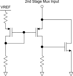
Each input to the multiplexer is clamped to prevent voltages on the port from exceeding the safe operating voltage of circuits attached to the system side of the port data multiplexer. Figure 11 shows the simplified clamping circuit. When a path through the multiplexer is closed, the clamp is connected to the one of the port pins (PA_USB_P/N, PB_USB_P/N). When a path through the multiplexer is not closed, then the port pin is not clamped. As the pin voltage rises above the VCLMP_IND voltage, the clamping circuit activates, and sinks current to ground, preventing the voltage from rising further.
 Figure 11. Port Mux Clamp