SLVSER3A November 2018 – April 2020 TPS65982BB
PRODUCTION DATA.
- 1 Features
- 2 Applications
- 3 Description
- 4 Revision History
- 5 Pin Configuration and Functions
-
6 Specifications
- 6.1 Absolute Maximum Ratings
- 6.2 ESD Ratings
- 6.3 Recommended Operating Conditions
- 6.4 Thermal Information
- 6.5 Power Supply Characteristics
- 6.6 Power Supervisor Characteristics
- 6.7 Power Consumption Characteristics
- 6.8 Port-Power Switch Characteristics
- 6.9 Port-Data Multiplexer Characteristics
- 6.10 Port-Data Multiplexer Clamp Characteristics
- 6.11 Port-Data Multiplexer Signal Monitoring Pullup and Pulldown Characteristics
- 6.12 USB Endpoint Characteristics
- 6.13 Input/Output (I/O) Characteristics
- 6.14 I2C Slave Characteristics
- 6.15 Thermal Shutdown Characteristics
- 6.16 Oscillator Characteristics
- 6.17 SPI Master Switching Characteristics
- 6.18 Typical Characteristics
- 7 Parameter Measurement Information
-
8 Detailed Description
- 8.1 Overview
- 8.2 Functional Block Diagram
- 8.3 Feature Description
- 8.4 Device Functional Modes
- 9 Application and Implementation
- 10Power Supply Recommendations
- 11Layout
- 12Device and Documentation Support
- 13Mechanical, Packaging, and Orderable Information
Package Options
Mechanical Data (Package|Pins)
- ZBH|96
Thermal pad, mechanical data (Package|Pins)
Orderable Information
8.3.3 Power Management
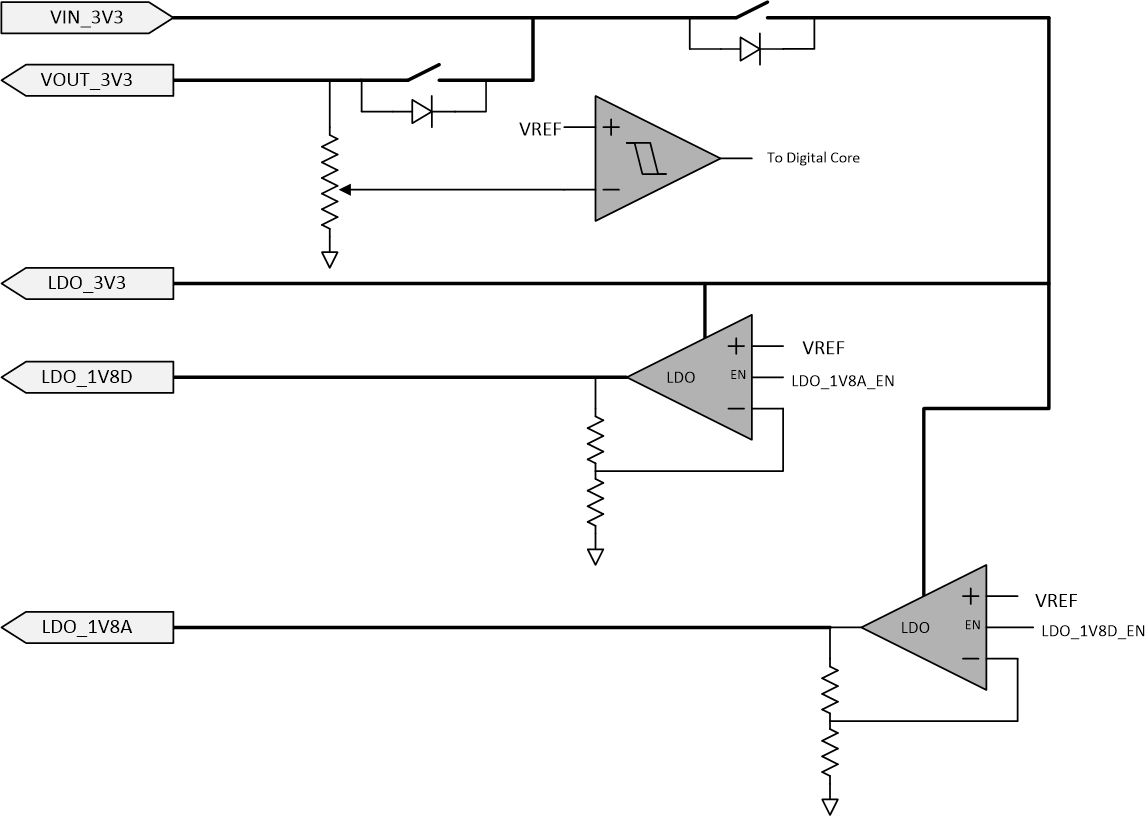
The TPS65982BB power management block receives power and generates voltages to provide power to the TPS65982BB internal circuitry. These generated power rails are LDO_3V3, LDO_1V8A, and LDO_1V8D. The LDO_3V3 power rail is also a low power output to load an optional external flash memory. The VOUT_3V3 power rail is a low-power output that does not power internal circuitry that is controlled by the application code and can be used to power other ICs in some applications. Figure 13 shows the power-supply path.
 Figure 13. Power Supply Path
 The TPS65982BB device is powered from VIN_3V3. Current flows from VIN_3V3 to LDO_3V3 to power the core 3.3-V circuitry and the 3.3-V I/Os. A second LDO steps the voltage down from LDO_3V3 to LDO_1V8D and LDO_1V8A to power the 1.8-V core digital circuitry and 1.8-V analog circuits.