SLVSER3A November 2018 – April 2020 TPS65982BB
PRODUCTION DATA.
- 1 Features
- 2 Applications
- 3 Description
- 4 Revision History
- 5 Pin Configuration and Functions
-
6 Specifications
- 6.1 Absolute Maximum Ratings
- 6.2 ESD Ratings
- 6.3 Recommended Operating Conditions
- 6.4 Thermal Information
- 6.5 Power Supply Characteristics
- 6.6 Power Supervisor Characteristics
- 6.7 Power Consumption Characteristics
- 6.8 Port-Power Switch Characteristics
- 6.9 Port-Data Multiplexer Characteristics
- 6.10 Port-Data Multiplexer Clamp Characteristics
- 6.11 Port-Data Multiplexer Signal Monitoring Pullup and Pulldown Characteristics
- 6.12 USB Endpoint Characteristics
- 6.13 Input/Output (I/O) Characteristics
- 6.14 I2C Slave Characteristics
- 6.15 Thermal Shutdown Characteristics
- 6.16 Oscillator Characteristics
- 6.17 SPI Master Switching Characteristics
- 6.18 Typical Characteristics
- 7 Parameter Measurement Information
-
8 Detailed Description
- 8.1 Overview
- 8.2 Functional Block Diagram
- 8.3 Feature Description
- 8.4 Device Functional Modes
- 9 Application and Implementation
- 10Power Supply Recommendations
- 11Layout
- 12Device and Documentation Support
- 13Mechanical, Packaging, and Orderable Information
Package Options
Mechanical Data (Package|Pins)
- ZBH|96
Thermal pad, mechanical data (Package|Pins)
Orderable Information
8.3.2.2 USB2.0 Low-Speed Endpoint
The USB low-speed endpoint is a USB 2.0 low-speed (1.5 Mbps) interface used to support HID class-based accesses. The TPS65982BB device supports control of endpoint EP0. This endpoint enumerates to a USB 2.0 bus to provide USB-Billboard information to a host system as defined in the USB Type-C standard. EP0 is used for advertising the Billboard Class. When a host is connected to a device that provides Alternate Modes that cannot be supported by the host, the Billboard class allows a means for the host to report back to the user without any silent failures.
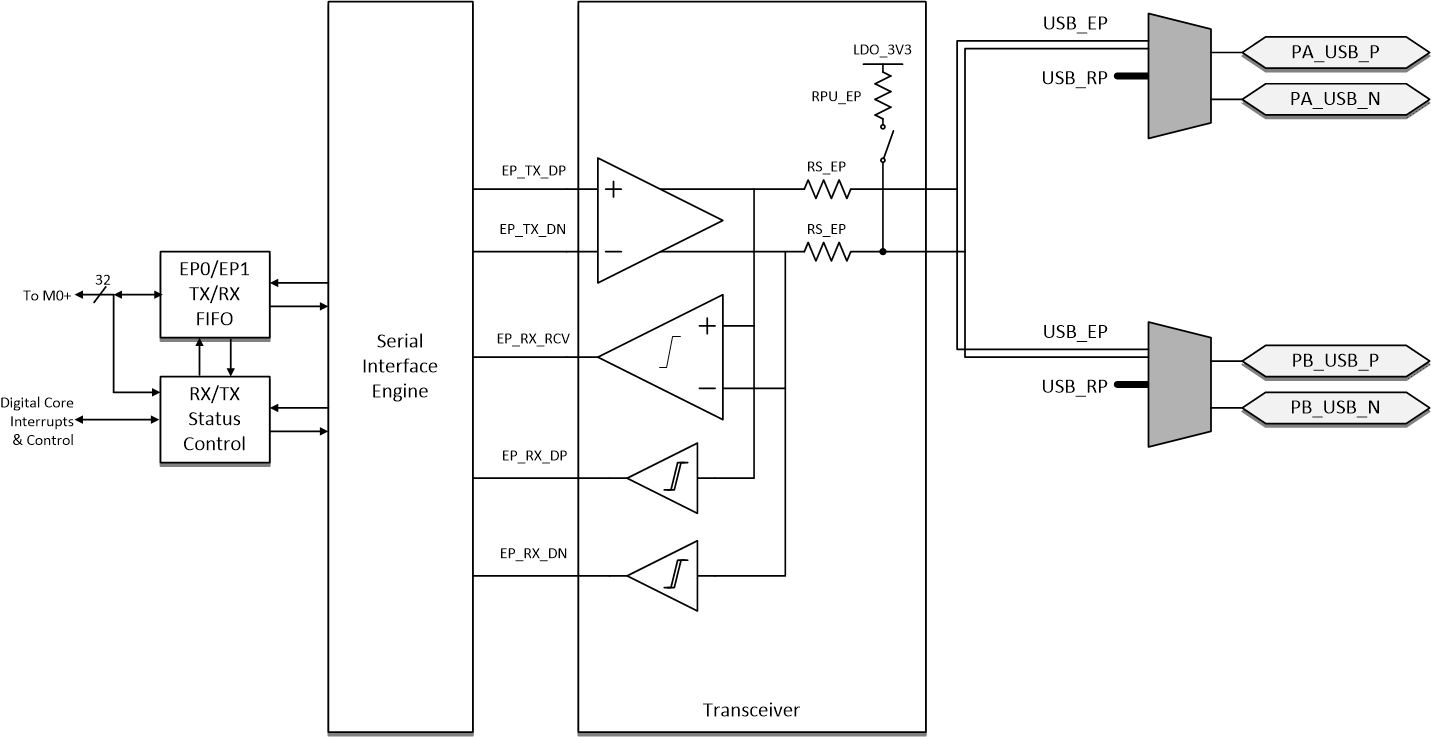
Figure 12 shows the physical layer of the USB endpoint. The physical layer consists of the analog transceiver, the serial interface engine, and the endpoint FIFOs. The physical layer supports low-speed operation.
 Figure 12. USB Endpoint PHY
 The transceiver is made up of a fully-differential output driver, a differential to single-ended receive buffer and two single-ended receive buffers on the D+/D– independently. The output driver drives the D+/D– of the selected output of the port multiplexer. The signals pass through the port-data multiplexer to the port pins. When driving, the signal is driven through a source resistance RS_EP. RS_EP is shown as a single resistor in the USB endpoint PHY but this resistance also includes the resistance of the port-data multiplexer defined in the Port-Data Multiplexer Characteristics table. RPU_EP is disconnected during transmit mode of the transceiver.
When the endpoint is in receive mode, the resistance RPU_EP is connected to the D– pin of the A or B port (PA_USB_N or PB_USB_N) depending on the detected orientation of the cable. The RPU_EP resistance advertises low-speed mode only.