SLVSFM6A August   2020  – July 2021 TPS65994AD

PRODUCTION DATA  

  1. Features
  2. Applications
  3. Description
  4. Revision History
  5. Pin Configuration and Functions
  6. Specifications
    1. 6.1  Absolute Maximum Ratings
    2. 6.2  ESD Ratings
    3. 6.3  Recommended Operating Conditions
    4. 6.4  Recommended Capacitance
    5. 6.5  Thermal Information
    6. 6.6  Power Supply Characteristics
    7. 6.7  Power Consumption
    8. 6.8  PP_5V Power Switch Characteristics
    9. 6.9  PP_EXT Power Switch Characteristics
    10. 6.10 Power Path Supervisory
    11. 6.11 CC Cable Detection Parameters
    12. 6.12 CC VCONN Parameters
    13. 6.13 CC PHY Parameters
    14. 6.14 Thermal Shutdown Characteristics
    15. 6.15 ADC Characteristics
    16. 6.16 Input/Output (I/O) Characteristics
    17. 6.17 I2C Requirements and Characteristics
    18. 6.18 Typical Characteristics
  7. Parameter Measurement Information
  8. Detailed Description
    1. 8.1 Overview
    2. 8.2 Functional Block Diagram
    3. 8.3 Feature Description
      1. 8.3.1  USB-PD Physical Layer
        1. 8.3.1.1 USB-PD Encoding and Signaling
        2. 8.3.1.2 USB-PD Bi-Phase Marked Coding
        3. 8.3.1.3 USB-PD Transmit (TX) and Receive (Rx) Masks
        4. 8.3.1.4 USB-PD BMC Transmitter
        5. 8.3.1.5 USB-PD BMC Receiver
        6. 8.3.1.6 Squelch Receiver
      2. 8.3.2  Power Management
        1. 8.3.2.1 Power-On And Supervisory Functions
        2. 8.3.2.2 VBUS LDO
      3. 8.3.3  Power Paths
        1. 8.3.3.1 Internal Sourcing Power Paths
          1. 8.3.3.1.1  PP_5Vx Current Clamping
          2. 8.3.3.1.2  PP_5Vx Local Overtemperature Shut Down (OTSD)
          3. 8.3.3.1.3  PP_5Vx Current Sense
          4. 8.3.3.1.4  PP_5Vx OVP
          5. 8.3.3.1.5  PP_5Vx UVLO
          6. 8.3.3.1.6  PP_5Vx Reverse Current Protection
          7. 8.3.3.1.7  Fast Role Swap
          8. 8.3.3.1.8  PP_CABLE Current Clamp
          9. 8.3.3.1.9  PP_CABLE Local Overtemperature Shut Down (OTSD)
          10. 8.3.3.1.10 PP_CABLE UVLO
        2. 8.3.3.2 Sink Path Control
          1. 8.3.3.2.1 Overvoltage Protection (OVP)
          2. 8.3.3.2.2 Reverse-Current Protection (RCP)
          3. 8.3.3.2.3 VBUS UVLO
          4. 8.3.3.2.4 Discharging VBUS to Safe Voltage
      4. 8.3.4  Cable Plug and Orientation Detection
        1. 8.3.4.1 Configured as a Source
        2. 8.3.4.2 Configured as a Sink
        3. 8.3.4.3 Configured as a DRP
        4. 8.3.4.4 Fast Role Swap Signal Detection
        5. 8.3.4.5 Dead Battery Advertisement
      5. 8.3.5  Default Behavior Configuration (ADCIN1, ADCIN2)
      6. 8.3.6  ADC
      7. 8.3.7  DisplayPort Hot-Plug Detect (HPD)
      8. 8.3.8  Digital Interfaces
        1. 8.3.8.1 General GPIO
        2. 8.3.8.2 I2C Interface
      9. 8.3.9  Digital Core
      10. 8.3.10 I2C Interface
        1. 8.3.10.1 I2C Interface Description
        2. 8.3.10.2 I2C Clock Stretching
        3. 8.3.10.3 I2C Address Setting
        4. 8.3.10.4 Unique Address Interface
    4. 8.4 Device Functional Modes
      1. 8.4.1 Pin Strapping to Configure Default Behavior
      2. 8.4.2 Power States
      3. 8.4.3 Thermal Shutdown
  9. Application and Implementation
    1. 9.1 Application Information
    2. 9.2 Typical Application
      1. 9.2.1 Type-C VBUS Design Considerations
        1. 9.2.1.1 Design Requirements
        2. 9.2.1.2 Detailed Design Procedure
          1. 9.2.1.2.1 Type-C Connector VBUS Capacitors
          2. 9.2.1.2.2 VBUS Schottky and TVS Diodes
        3. 9.2.1.3 Application Curves
      2. 9.2.2 Notebook Design Supporting PD Charging
        1. 9.2.2.1 USB and DisplayPort Notebook Supporting PD Charging
          1. 9.2.2.1.1 Design Requirements
          2. 9.2.2.1.2 Detailed Design Procedure
            1. 9.2.2.1.2.1 USB Power Delivery Source Capabilities
            2. 9.2.2.1.2.2 USB Power Delivery Sink Capabilities
            3. 9.2.2.1.2.3 USB and DisplayPort Supported Data Modes
            4. 9.2.2.1.2.4 TUSB1046 Super Speed Mux GPIO Control
        2. 9.2.2.2 Thunderbolt Notebook Supporting PD Charging
          1. 9.2.2.2.1 Design Requirements
          2. 9.2.2.2.2 Detailed Design Procedure
            1. 9.2.2.2.2.1 USB Power Delivery Source Capabilities
            2. 9.2.2.2.2.2 USB Power Delivery Sink Capabilities
            3. 9.2.2.2.2.3 Thunderbolt Supported Data Modes
            4. 9.2.2.2.2.4 I2C Design Requirements
            5. 9.2.2.2.2.5 TS3DS10224 SBU Mux for AUX and LSTX/RX
  10. 10Power Supply Recommendations
    1. 10.1 3.3-V Power
      1. 10.1.1 VIN_3V3 Input Switch
      2. 10.1.2 VBUS 3.3-V LDO
    2. 10.2 1.5-V Power
    3. 10.3 Recommended Supply Load Capacitance
  11. 11Layout
    1. 11.1 Layout Guidelines
      1. 11.1.1 Top TPS65994AD Placement and Bottom Component Placement and Layout
    2. 11.2 Layout Example
    3. 11.3 Component Placement
    4. 11.4 Routing PP_5V, VBUS, VIN_3V3, LDO_3V3, LDO_1V5
    5. 11.5 Routing CC and GPIO
  12. 12Device and Documentation Support
    1. 12.1 Device Support
      1. 12.1.1 Third-Party Products Disclaimer
    2. 12.2 Documentation Support
      1. 12.2.1 Related Documentation
    3. 12.3 Support Resources
    4. 12.4 Trademarks
    5. 12.5 Electrostatic Discharge Caution
    6. 12.6 Glossary
  13. 13Mechanical, Packaging, and Orderable Information
    1. 13.1 Package Option Addendum
      1. 13.1.1 Tape and Reel Information

Package Options

Refer to the PDF data sheet for device specific package drawings

Mechanical Data (Package|Pins)
  • RSL|48
Thermal pad, mechanical data (Package|Pins)
Orderable Information

Description

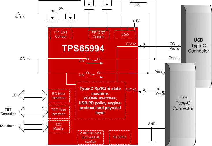
The TPS65994AD is a highly integrated stand-alone Dual Port USB Type-C and Power Delivery (PD) controller for PC and notebooks applications. The TPS65994AD integrates fully managed source paths with robust protection for a complete USB-C PD solution. TPS65994AD is featured on Intel and AMD’s Reference Design for PC and notebook end equipment ensuring the PD controller has proper system level interaction in these types of designs. This feature greatly reduces system design complexity and results in reduced time to market.

Device Information
PART NUMBER(1)PACKAGEBODY SIZE (NOM)
TPS65994ADQFN (RSL)6.0 mm x 6.0 mm
For all available packages, see the orderable addendum at the end of the data sheet.
GUID-EF60963C-7AD8-4268-939F-B1B7E4B9020A-low.gif