SBVS087M June   2008  – June 2018 TPS735

PRODUCTION DATA.  

  1. Features
  2. Applications
  3. Description
    1.     Typical Application
  4. Revision History
    1.     Pin Configuration and Functions
      1.      Pin Functions
  5. Specifications
    1. 5.1 Absolute Maximum Ratings
    2. 5.2 ESD Ratings
    3. 5.3 Recommended Operating Conditions
    4. 5.4 Thermal Information
    5. 5.5 Electrical Characteristics
    6. 5.6 Typical Characteristics
  6. Detailed Description
    1. 6.1 Overview
    2. 6.2 Functional Block Diagrams
    3. 6.3 Feature Description
      1. 6.3.1 Internal Current Limit
      2. 6.3.2 Shutdown
      3. 6.3.3 Dropout Voltage
      4. 6.3.4 Start-Up and Noise Reduction Capacitor
      5. 6.3.5 Transient Response
      6. 6.3.6 Undervoltage Lockout
      7. 6.3.7 Minimum Load
      8. 6.3.8 Thermal Protection
    4. 6.4 Device Functional Modes
      1. 6.4.1 Normal Operation
      2. 6.4.2 Dropout Operation
      3. 6.4.3 Disabled
  7. Application and Implementation
    1. 7.1 Application Information
    2. 7.2 Typical Applications
      1. 7.2.1 Design Requirements
        1. 7.2.1.1 Input and Output Capacitor Requirements
        2. 7.2.1.2 Feed-Forward Capacitor Requirements
      2. 7.2.2 Detailed Design Procedure
        1. 7.2.2.1 Output Noise
      3. 7.2.3 Application Curves
  8. Power Supply Recommendations
  9. Layout
    1. 9.1 Layout Guidelines
      1. 9.1.1 Board Layout Recommendations to Improve PSRR and Noise Performance
    2. 9.2 Layout Example
    3. 9.3 Power Dissipation
    4. 9.4 Estimating Junction Temperature
    5. 9.5 Package Mounting
  10. 10Device and Documentation Support
    1. 10.1 Device Support
      1. 10.1.1 Development Support
        1. 10.1.1.1 Evaluation Modules
      2. 10.1.2 Device Nomenclature
    2. 10.2 Documentation Support
      1. 10.2.1 Related Documentation
    3. 10.3 Trademarks
    4. 10.4 Electrostatic Discharge Caution
    5. 10.5 Glossary
  11. 11Mechanical, Packaging, and Orderable Information

Package Options

Mechanical Data (Package|Pins)
Thermal pad, mechanical data (Package|Pins)
Orderable Information

Application Curves

at VIN = VOUT(nom) + 0.5 V or 2.7 V, whichever is greater; IOUT = 1 mA, VEN = VIN, COUT = 2.2 μF, CNR = 10 nF, and TJ = 25°C (unless otherwise noted)

TPS735 tc_turn_on_resp_sbvs252.gif
Figure 17. TPS735 Turnon Response (VIN = VEN)
TPS735 tc_pupd_sbvs252.gif
RL = 5 Ω
Figure 19. TPS73525 Power-Up and Power-Down
(VIN = VEN)
TPS735 tc_line_tr_sbvs252.gif
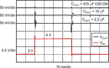
Figure 21. TPS735 Line Transient Response
TPS735 tc_enable_resp_vin_sbvs252.gif
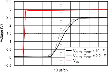
Figure 18. TPS735 Turnon Response Using EN
TPS735 tc_load_tr_sbvs252.gif
VIN = 3 V
Figure 20. TPS735 Load Transient Response