SBVS066S December   2005  – November 2024 TPS74401

PRODUCTION DATA  

  1.   1
  2. Features
  3. Applications
  4. Description
  5. Pin Configuration and Functions
  6. Specifications
    1. 5.1 Absolute Maximum Ratings
    2. 5.2 ESD Ratings
    3. 5.3 Recommended Operating Conditions
    4. 5.4 Thermal Information
    5. 5.5 Electrical Characteristics
    6. 5.6 Typical Characteristics
  7. Detailed Description
    1. 6.1 Overview
    2. 6.2 Functional Block Diagram
    3. 6.3 Feature Description
      1. 6.3.1 Enable, Shutdown
      2. 6.3.2 Power-Good (VQFN Package Only)
      3. 6.3.3 Internal Current Limit
      4. 6.3.4 Thermal Protection
    4. 6.4 Device Functional Modes
      1. 6.4.1 Normal Operation
      2. 6.4.2 Dropout Operation
      3. 6.4.3 Disabled
    5. 6.5 Programming
      1. 6.5.1 Programmable Soft-Start
      2. 6.5.2 Sequencing Requirements
  8. Application and Implementation
    1. 7.1 Application Information
      1. 7.1.1 Input, Output, and Bias Capacitor Requirements
      2. 7.1.2 Transient Response
      3. 7.1.3 Dropout Voltage
      4. 7.1.4 Output Noise
    2. 7.2 Typical Applications
      1. 7.2.1 Setting the TPS74401
        1. 7.2.1.1 Design Requirements
        2. 7.2.1.2 Detailed Design Procedure
        3. 7.2.1.3 Application Curves
      2. 7.2.2 Using an Auxiliary Bias Rail
      3. 7.2.3 Without an Auxiliary Bias
    3. 7.3 Power Supply Recommendations
    4. 7.4 Layout
      1. 7.4.1 Layout Guidelines
        1. 7.4.1.1 Power Dissipation
        2. 7.4.1.2 Thermal Considerations
      2. 7.4.2 Layout Example
  9. Device and Documentation Support
    1. 8.1 Documentation Support
      1. 8.1.1 Related Documentation
      2. 8.1.2 Device Nomenclature
    2. 8.2 Device Support
      1. 8.2.1 Development Support
        1. 8.2.1.1 Evaluation Modules
        2. 8.2.1.2 Spice Models
    3. 8.3 Receiving Notification of Documentation Updates
    4. 8.4 Support Resources
    5. 8.5 Trademarks
    6. 8.6 Electrostatic Discharge Caution
    7. 8.7 Glossary
  10. Revision History
  11. 10Mechanical, Packaging, and Orderable Information

Package Options

Mechanical Data (Package|Pins)
Thermal pad, mechanical data (Package|Pins)
Orderable Information

Description

The TPS74401 low-dropout (LDO) linear regulators provide an easy-to-use robust power-management option for a wide variety of applications. The user-programmable soft-start minimizes stress on the input power source by reducing capacitive inrush current on start-up. The soft-start is monotonic and designed for powering many different types of processors and application-specific integrated circuits (ASICs). The enable input and power-good output allow easy sequencing with external regulators. Complete flexibility lets the user configure a plan that meets the sequencing requirements of field-programmable gate arrays (FPGAs), digital signal processors (DSPs), and other applications with specific start-up requirements.

A precision reference and error amplifier deliver 1% accuracy over load, line, temperature, and process. The device is stable without an output capacitor (legacy chip) or with any type of capacitor ≥ 2.2µF (new chip). The device is fully specified from TJ = –40°C to 125°C.

Package Information
PART NUMBER PACKAGE(1) PACKAGE SIZE(2)
TPS74401 KTW (TO-263, 7) 10.1mm × 15.24mm
RGR (VQFN, 20) 3.5mm × 3.5mm
RGW (VQFN, 20) 5mm × 5mm
For more information, see the Mechanical, Packaging, and Orderable Information.
The package size (length × width) is a nominal value and includes pins, where applicable.
TPS74401 Typical Application CircuitTypical Application Circuit
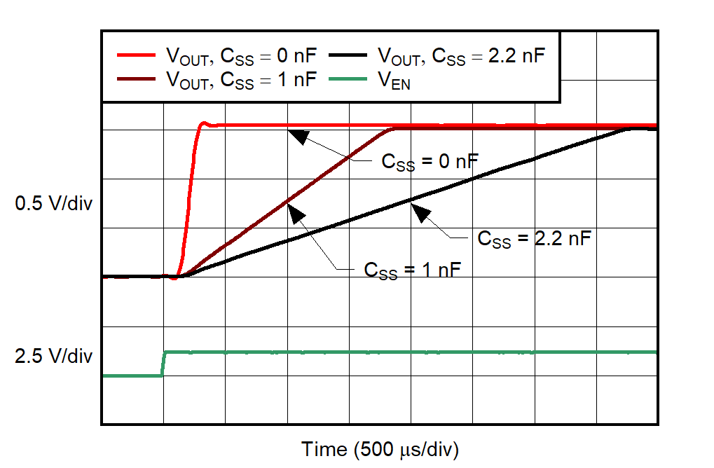
TPS74401 Turn-On ResponseTurn-On Response