SBVS066S December   2005  – November 2024 TPS74401

PRODUCTION DATA  

  1.   1
  2. Features
  3. Applications
  4. Description
  5. Pin Configuration and Functions
  6. Specifications
    1. 5.1 Absolute Maximum Ratings
    2. 5.2 ESD Ratings
    3. 5.3 Recommended Operating Conditions
    4. 5.4 Thermal Information
    5. 5.5 Electrical Characteristics
    6. 5.6 Typical Characteristics
  7. Detailed Description
    1. 6.1 Overview
    2. 6.2 Functional Block Diagram
    3. 6.3 Feature Description
      1. 6.3.1 Enable, Shutdown
      2. 6.3.2 Power-Good (VQFN Package Only)
      3. 6.3.3 Internal Current Limit
      4. 6.3.4 Thermal Protection
    4. 6.4 Device Functional Modes
      1. 6.4.1 Normal Operation
      2. 6.4.2 Dropout Operation
      3. 6.4.3 Disabled
    5. 6.5 Programming
      1. 6.5.1 Programmable Soft-Start
      2. 6.5.2 Sequencing Requirements
  8. Application and Implementation
    1. 7.1 Application Information
      1. 7.1.1 Input, Output, and Bias Capacitor Requirements
      2. 7.1.2 Transient Response
      3. 7.1.3 Dropout Voltage
      4. 7.1.4 Output Noise
    2. 7.2 Typical Applications
      1. 7.2.1 Setting the TPS74401
        1. 7.2.1.1 Design Requirements
        2. 7.2.1.2 Detailed Design Procedure
        3. 7.2.1.3 Application Curves
      2. 7.2.2 Using an Auxiliary Bias Rail
      3. 7.2.3 Without an Auxiliary Bias
    3. 7.3 Power Supply Recommendations
    4. 7.4 Layout
      1. 7.4.1 Layout Guidelines
        1. 7.4.1.1 Power Dissipation
        2. 7.4.1.2 Thermal Considerations
      2. 7.4.2 Layout Example
  9. Device and Documentation Support
    1. 8.1 Documentation Support
      1. 8.1.1 Related Documentation
      2. 8.1.2 Device Nomenclature
    2. 8.2 Device Support
      1. 8.2.1 Development Support
        1. 8.2.1.1 Evaluation Modules
        2. 8.2.1.2 Spice Models
    3. 8.3 Receiving Notification of Documentation Updates
    4. 8.4 Support Resources
    5. 8.5 Trademarks
    6. 8.6 Electrostatic Discharge Caution
    7. 8.7 Glossary
  10. Revision History
  11. 10Mechanical, Packaging, and Orderable Information

Package Options

Mechanical Data (Package|Pins)
Thermal pad, mechanical data (Package|Pins)
Orderable Information

Setting the TPS74401

Figure 7-1 shows a typical application circuit for the TPS74401.

R1 and R2 can be calculated for any output voltage using the formula shown in Figure 7-1. Table 7-1 lists sample resistor values of common output voltages. To achieve the maximum accuracy specifications, R2 must be ≤ 4.99kΩ.
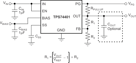
TPS74401 Typical Application Circuit for the TPS74401Figure 7-1 Typical Application Circuit for the TPS74401
Table 7-1 Standard 1% Resistor Values for Programming the Output Voltage
R1 (kΩ) R2 (kΩ) VOUT (V)(1)
Short Open 0.8
0.619 4.99 0.9
1.13 4.53 1.0
1.37 4.42 1.05
1.87 4.99 1.1
2.49 4.99 1.2
4.12 4.75 1.5
3.57 2.87 1.8
3.57 1.69 2.5
3.57 1.15 3.3
V O U T = 0.8 × 1 + R 1 ÷ R 2
Note:

When VBIAS and VEN are present and VIN is not supplied, this device outputs approximately 50μA of current from OUT. Although this condition does not cause any damage to the device, the output current can charge up the OUT node if total resistance between OUT and GND (including external feedback resistors) is greater than 10kΩ.