SBVS387C February   2020  – January 2022 TPS784-Q1

PRODUCTION DATA  

  1. Features
  2. Applications
  3. Description
  4. Revision History
  5. Pin Configuration and Functions
  6. Specifications
    1. 6.1 Absolute Maximum Ratings
    2. 6.2 ESD Ratings
    3. 6.3 Recommended Operating Conditions
    4. 6.4 Thermal Information
    5. 6.5 Electrical Characteristics
    6. 6.6 Typical Characteristics
  7. Detailed Description
    1. 7.1 Overview
    2. 7.2 Functional Block Diagrams
    3. 7.3 Feature Description
      1. 7.3.1 Foldback Current Limit
      2. 7.3.2 Output Enable
      3. 7.3.3 Active Discharge
      4. 7.3.4 Undervoltage Lockout (UVLO) Operation
      5. 7.3.5 Dropout Voltage
      6. 7.3.6 Thermal Shutdown
    4. 7.4 Device Functional Modes
      1. 7.4.1 Device Functional Mode Comparison
      2. 7.4.2 Normal Operation
      3. 7.4.3 Dropout Operation
      4. 7.4.4 Disabled
  8. Application and Implementation
    1. 8.1 Application Information
      1. 8.1.1 Recommended Capacitor Types
      2. 8.1.2 Input and Output Capacitor Requirements
      3. 8.1.3 Adjustable Device Feedback Resistors
      4. 8.1.4 Load Transient Response
      5. 8.1.5 Exiting Dropout
      6. 8.1.6 Dropout Voltage
      7. 8.1.7 Reverse Current
      8. 8.1.8 Feed-Forward Capacitor (CFF)
      9. 8.1.9 Power Dissipation (PD)
        1. 8.1.9.1 Estimating Junction Temperature
        2. 8.1.9.2 Recommended Area for Continuous Operation
        3. 8.1.9.3 Power Dissipation versus Ambient Temperature
    2. 8.2 Typical Application
      1. 8.2.1 Design Requirements
      2. 8.2.2 Detailed Design Procedure
      3. 8.2.3 Application Curves
  9. Power Supply Recommendations
  10. 10Layout
    1. 10.1 Layout Guidelines
      1. 10.1.1 Additional Layout Considerations
    2. 10.2 Layout Examples
  11. 11Device and Documentation Support
    1. 11.1 Device Support
      1. 11.1.1 Device Nomenclature
    2. 11.2 Documentation Support
      1. 11.2.1 Related Documentation
    3. 11.3 Receiving Notification of Documentation Updates
    4. 11.4 Support Resources
    5. 11.5 Trademarks
    6. 11.6 Electrostatic Discharge Caution
    7. 11.7 Glossary
  12. 12Mechanical, Packaging, and Orderable Information

Package Options

Mechanical Data (Package|Pins)
Thermal pad, mechanical data (Package|Pins)
Orderable Information

Description

The TPS784-Q1 ultra low-dropout regulator (LDO) is a small, low quiescent current LDO that can source 300 mA with excellent line and load transient performance.

The low output noise and great PSRR performance make the device suitable to power sensitive analog loads. The TPS784-Q1 is a flexible device for post regulation because this device supports an input voltage range from 1.65 V to 6.0 V and offers an adjustable output range of 1.2 V to 5.5 V. The device also features fixed output voltages from 0.65 V to 5.0 V for powering common voltage rails.

The TPS784-Q1 offers foldback current limit to reduce power dissipation during over current condition. The EN input helps with power sequencing requirements of the system. The internal soft-start provides a controlled start up, reducing the inrush current and allowing for lower input capacitance to be used.

The TPS784-Q1 provides an active pulldown circuit to quickly discharge output loads when disabled.

Device Information(1)
PART NUMBER PACKAGE BODY SIZE (NOM)
TPS784-Q1 Wettable flank VSON (8) 3.00 mm × 3.00 mm
SOT-23 (5) 2.90 mm × 1.60 mm
For all available packages, see the orderable addendum at the end of the data sheet.
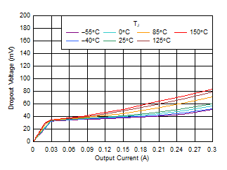
GUID-20200820-CA0I-MWL6-ZSDR-V0T131VLMBVX-low.gifDropout vs IOUT for 5.0 V
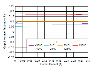
GUID-842214BB-638B-4950-A8DF-EE6BA4289DAF-low.gifOutput Accuracy vs IOUT for 5.0 V