SBVS387C February   2020  – January 2022 TPS784-Q1

PRODUCTION DATA  

  1. Features
  2. Applications
  3. Description
  4. Revision History
  5. Pin Configuration and Functions
  6. Specifications
    1. 6.1 Absolute Maximum Ratings
    2. 6.2 ESD Ratings
    3. 6.3 Recommended Operating Conditions
    4. 6.4 Thermal Information
    5. 6.5 Electrical Characteristics
    6. 6.6 Typical Characteristics
  7. Detailed Description
    1. 7.1 Overview
    2. 7.2 Functional Block Diagrams
    3. 7.3 Feature Description
      1. 7.3.1 Foldback Current Limit
      2. 7.3.2 Output Enable
      3. 7.3.3 Active Discharge
      4. 7.3.4 Undervoltage Lockout (UVLO) Operation
      5. 7.3.5 Dropout Voltage
      6. 7.3.6 Thermal Shutdown
    4. 7.4 Device Functional Modes
      1. 7.4.1 Device Functional Mode Comparison
      2. 7.4.2 Normal Operation
      3. 7.4.3 Dropout Operation
      4. 7.4.4 Disabled
  8. Application and Implementation
    1. 8.1 Application Information
      1. 8.1.1 Recommended Capacitor Types
      2. 8.1.2 Input and Output Capacitor Requirements
      3. 8.1.3 Adjustable Device Feedback Resistors
      4. 8.1.4 Load Transient Response
      5. 8.1.5 Exiting Dropout
      6. 8.1.6 Dropout Voltage
      7. 8.1.7 Reverse Current
      8. 8.1.8 Feed-Forward Capacitor (CFF)
      9. 8.1.9 Power Dissipation (PD)
        1. 8.1.9.1 Estimating Junction Temperature
        2. 8.1.9.2 Recommended Area for Continuous Operation
        3. 8.1.9.3 Power Dissipation versus Ambient Temperature
    2. 8.2 Typical Application
      1. 8.2.1 Design Requirements
      2. 8.2.2 Detailed Design Procedure
      3. 8.2.3 Application Curves
  9. Power Supply Recommendations
  10. 10Layout
    1. 10.1 Layout Guidelines
      1. 10.1.1 Additional Layout Considerations
    2. 10.2 Layout Examples
  11. 11Device and Documentation Support
    1. 11.1 Device Support
      1. 11.1.1 Device Nomenclature
    2. 11.2 Documentation Support
      1. 11.2.1 Related Documentation
    3. 11.3 Receiving Notification of Documentation Updates
    4. 11.4 Support Resources
    5. 11.5 Trademarks
    6. 11.6 Electrostatic Discharge Caution
    7. 11.7 Glossary
  12. 12Mechanical, Packaging, and Orderable Information

Package Options

Mechanical Data (Package|Pins)
Thermal pad, mechanical data (Package|Pins)
Orderable Information

Additional Layout Considerations

The high impedance of the FB pin makes the regulator sensitive to parasitic capacitances that may couple undesirable signals from nearby components (especially from logic and digital devices, such as microcontrollers and microprocessors); these capacitively-coupled signals may produce undesirable output voltage transients. In these cases, TI recommends using a fixed-voltage version of the device, or isolating the FB node by placing a copper ground plane on the layer directly underneath the LDO circuitry and FB pin to minimize any undesirable signal coupling.

GUID-20200820-CA0I-B2CV-0VLZ-CXR5GHF8ZCBV-low.gif
4-layer PCB
Figure 10-1 Junction-to-Ambient Thermal Resistance (RθJA) vs PCB Copper Area
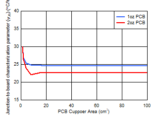
GUID-20200820-CA0I-HG2F-3W6W-RJVR5BSDVPZC-low.gif
4-layer PCB
Figure 10-3 Junction-to-Board Characterization Parameter (ψJB) vs PCB Copper Area
GUID-20200820-CA0I-0GN6-XFQD-GLRGNWCRMFLM-low.gif
2-layer PCB
Figure 10-2 Junction-to-Ambient Thermal Resistance (RθJA) vs PCB Copper Area
GUID-20200820-CA0I-QZD7-FDLP-8S0LJZSJ9JCP-low.gif
2-layer PCB
Figure 10-4 Junction-to-Board Characterization Parameter (ψJB) vs PCB Copper Area