SBVS387C February   2020  – January 2022 TPS784-Q1

PRODUCTION DATA  

  1. Features
  2. Applications
  3. Description
  4. Revision History
  5. Pin Configuration and Functions
  6. Specifications
    1. 6.1 Absolute Maximum Ratings
    2. 6.2 ESD Ratings
    3. 6.3 Recommended Operating Conditions
    4. 6.4 Thermal Information
    5. 6.5 Electrical Characteristics
    6. 6.6 Typical Characteristics
  7. Detailed Description
    1. 7.1 Overview
    2. 7.2 Functional Block Diagrams
    3. 7.3 Feature Description
      1. 7.3.1 Foldback Current Limit
      2. 7.3.2 Output Enable
      3. 7.3.3 Active Discharge
      4. 7.3.4 Undervoltage Lockout (UVLO) Operation
      5. 7.3.5 Dropout Voltage
      6. 7.3.6 Thermal Shutdown
    4. 7.4 Device Functional Modes
      1. 7.4.1 Device Functional Mode Comparison
      2. 7.4.2 Normal Operation
      3. 7.4.3 Dropout Operation
      4. 7.4.4 Disabled
  8. Application and Implementation
    1. 8.1 Application Information
      1. 8.1.1 Recommended Capacitor Types
      2. 8.1.2 Input and Output Capacitor Requirements
      3. 8.1.3 Adjustable Device Feedback Resistors
      4. 8.1.4 Load Transient Response
      5. 8.1.5 Exiting Dropout
      6. 8.1.6 Dropout Voltage
      7. 8.1.7 Reverse Current
      8. 8.1.8 Feed-Forward Capacitor (CFF)
      9. 8.1.9 Power Dissipation (PD)
        1. 8.1.9.1 Estimating Junction Temperature
        2. 8.1.9.2 Recommended Area for Continuous Operation
        3. 8.1.9.3 Power Dissipation versus Ambient Temperature
    2. 8.2 Typical Application
      1. 8.2.1 Design Requirements
      2. 8.2.2 Detailed Design Procedure
      3. 8.2.3 Application Curves
  9. Power Supply Recommendations
  10. 10Layout
    1. 10.1 Layout Guidelines
      1. 10.1.1 Additional Layout Considerations
    2. 10.2 Layout Examples
  11. 11Device and Documentation Support
    1. 11.1 Device Support
      1. 11.1.1 Device Nomenclature
    2. 11.2 Documentation Support
      1. 11.2.1 Related Documentation
    3. 11.3 Receiving Notification of Documentation Updates
    4. 11.4 Support Resources
    5. 11.5 Trademarks
    6. 11.6 Electrostatic Discharge Caution
    7. 11.7 Glossary
  12. 12Mechanical, Packaging, and Orderable Information

Package Options

Mechanical Data (Package|Pins)
Thermal pad, mechanical data (Package|Pins)
Orderable Information

Application Curves

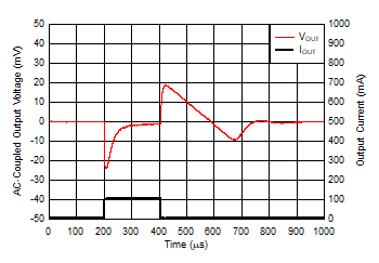
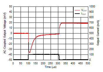
A 10-µF capacitor is used to reduce overshoot and undershoot of output voltage during load transients with ramps rates greater than 0.5 A/µs. Figure 8-9 and Figure 8-10 show captures of load transient behavior for this application.
GUID-0C1C4A60-065E-4990-8D42-2E30CDF91D5F-low.gif
VIN = 3.8 V, VOUT = 3.3 V, COUT = 10 µF,
IOUT slew rate = 1 A/µs
Figure 8-9 IOUT Transient From 0 mA to 100 mA
GUID-9099E63C-E754-461B-B562-145E5E891FB9-low.gif
VIN = 3.8 V, VOUT = 3.3 V, COUT = 10 µF,
IOUT slew rate = 1 A/µs
Figure 8-10 IOUT Transient From 1 mA to 100 mA