SBVS400D december 2021 – august 2023 TPS7A14
PRODUCTION DATA
- 1
- 1Features
- 2Applications
- 3Description
- 4Revision History
- 5Pin Configuration and Functions
- 6Specifications
- 7Detailed Description
-
8Application and Implementation
- 8.1
Application Information
- 8.1.1 Recommended Capacitor Types
- 8.1.2 Input, Output, and Bias Capacitor Requirements
- 8.1.3 Dropout Voltage
- 8.1.4 Behavior During Transition From Dropout Into Regulation
- 8.1.5 Device Enable Sequencing Requirement
- 8.1.6 Load Transient Response
- 8.1.7 Undervoltage Lockout Circuit Operation
- 8.1.8 Power Dissipation (PD)
- 8.1.9 Estimating Junction Temperature
- 8.1.10 Recommended Area for Continuous Operation
- 8.2 Typical Application
- 8.3 Power Supply Recommendations
- 8.4 Layout
- 8.1
Application Information
- 9Device and Documentation Support
- Mechanical, Packaging, and Orderable Information
Package Options
Mechanical Data (Package|Pins)
- DRV|6
- YBK|6
Thermal pad, mechanical data (Package|Pins)
- DRV|6
Orderable Information
7.3.4 Internal Foldback Current Limit
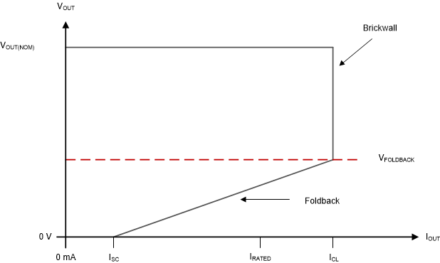
The device has an internal current limit circuit that protects the regulator during transient high-load current faults or shorting events. The current limit is a hybrid brick-wall foldback scheme. The current limit transitions from a brick-wall scheme to a foldback scheme at the foldback voltage (VFOLDBACK). In a high-load current fault with the output voltage above VFOLDBACK, the brick-wall scheme limits the output current to the current limit (ICL). When the voltage drops below VFOLDBACK, a foldback current limit activates that scales back the current as the output voltage approaches GND. When the output is shorted, the device supplies a typical current called the short-circuit current limit (ISC). ICL and ISC are listed in the Electrical CharacteristicsElectrical CharacteristicsElectrical CharacteristicsElectrical CharacteristicsElectrical Characteristics table.
For this device, VFOLDBACK is approximately 60% × VOUT(nom).
The output voltage is not regulated when the device is in current limit. When a current limit event occurs, the device begins to heat up because of the increase in power dissipation. When the device is in brick-wall current limit, the pass transistor dissipates power [(VIN – VOUT) × ICL]. When the device output is shorted and the output is below VFOLDBACK, the pass transistor dissipates power [(VIN – VOUT) × ISC]. If thermal shutdown is triggered, the device turns off. After the device cools down, the internal thermal shutdown circuit turns the device back on. If the output current fault condition continues, the device cycles between current limit and thermal shutdown. For more information on current limits, see the Know Your Limits application report.
Figure 7-2 shows a diagram of the foldback current limit.
 Figure 7-2 Foldback Current Limit