SLVSD43C May 2015 – February 2019 TPS7B68-Q1
PRODUCTION DATA.
- 1 Features
- 2 Applications
- 3 Description
- 4 Revision History
- 5 Pin Configuration and Functions
- 6 Specifications
-
7 Detailed Description
- 7.1 Overview
- 7.2 Functional Block Diagram
- 7.3
Feature Description
- 7.3.1 Device Enable (EN)
- 7.3.2 Adjustable Power-Good Threshold (PG, PGADJ)
- 7.3.3 Adjustable Power-Good Delay Timer (DELAY)
- 7.3.4 Undervoltage Shutdown
- 7.3.5 Current Limit
- 7.3.6 Thermal Shutdown
- 7.3.7
Integrated Watchdog
- 7.3.7.1 Window Watchdog (WTS, ROSC, FSEL and WRS)
- 7.3.7.2 Standard Watchdog (WTS, ROSC and FSEL)
- 7.3.7.3 Watchdog Service Signal and Watchdog Fault Outputs (WD and WDO)
- 7.3.7.4 ROSC Status Detection (ROSC)
- 7.3.7.5 Watchdog Enable (PG and WD_EN)
- 7.3.7.6 Watchdog Initialization
- 7.3.7.7 Window Watchdog Operation (WTS = Low)
- 7.3.7.8 Standard Watchdog Operation (WTS = High)
- 7.4 Device Functional Modes
- 8 Application and Implementation
- 9 Power Supply Recommendations
- 10Layout
- 11Device and Documentation Support
- 12Mechanical, Packaging, and Orderable Information
Package Options
Mechanical Data (Package|Pins)
- PWP|28
Thermal pad, mechanical data (Package|Pins)
- PWP|28
Orderable Information
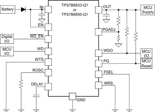
8.2 Typical Application
Figure 26 shows a typical application circuit for the TPS7B68-Q1. Different values of external components can be used, depending on the end application. An application may require a larger output capacitor during fast load steps to prevent a large drop on the output voltage. TI recommends using a low-ESR ceramic capacitor with a dielectric of type X7R.
 Figure 26. TPS7B68-Q1 Typical Application Schematic