SLVSD43C May   2015  – February 2019 TPS7B68-Q1

PRODUCTION DATA.  

  1. Features
  2. Applications
  3. Description
    1.     Typical Application Schematic
  4. Revision History
  5. Pin Configuration and Functions
    1.     Pin Functions
  6. Specifications
    1. 6.1 Absolute Maximum Ratings
    2. 6.2 ESD Ratings
    3. 6.3 Recommended Operating Conditions
    4. 6.4 Thermal Information
    5. 6.5 Electrical Characteristics
    6. 6.6 Switching Characteristics
    7. 6.7 Typical Characteristics
  7. Detailed Description
    1. 7.1 Overview
    2. 7.2 Functional Block Diagram
    3. 7.3 Feature Description
      1. 7.3.1 Device Enable (EN)
      2. 7.3.2 Adjustable Power-Good Threshold (PG, PGADJ)
      3. 7.3.3 Adjustable Power-Good Delay Timer (DELAY)
      4. 7.3.4 Undervoltage Shutdown
      5. 7.3.5 Current Limit
      6. 7.3.6 Thermal Shutdown
      7. 7.3.7 Integrated Watchdog
        1. 7.3.7.1 Window Watchdog (WTS, ROSC, FSEL and WRS)
        2. 7.3.7.2 Standard Watchdog (WTS, ROSC and FSEL)
        3. 7.3.7.3 Watchdog Service Signal and Watchdog Fault Outputs (WD and WDO)
        4. 7.3.7.4 ROSC Status Detection (ROSC)
        5. 7.3.7.5 Watchdog Enable (PG and WD_EN)
        6. 7.3.7.6 Watchdog Initialization
        7. 7.3.7.7 Window Watchdog Operation (WTS = Low)
        8. 7.3.7.8 Standard Watchdog Operation (WTS = High)
    4. 7.4 Device Functional Modes
      1. 7.4.1 Operation With Input Voltage Lower Than 4 V
      2. 7.4.2 Operation With Input Voltage Higher Than 4 V
  8. Application and Implementation
    1. 8.1 Application Information
    2. 8.2 Typical Application
      1. 8.2.1 Design Requirements
      2. 8.2.2 Detailed Design Procedure
        1. 8.2.2.1 Input Capacitor
        2. 8.2.2.2 Output Capacitor
        3. 8.2.2.3 Power-Good Threshold
        4. 8.2.2.4 Power-Good Delay Period
        5. 8.2.2.5 Watchdog Setup
      3. 8.2.3 Application Curves
  9. Power Supply Recommendations
  10. 10Layout
    1. 10.1 Layout Guidelines
    2. 10.2 Layout Example
  11. 11Device and Documentation Support
    1. 11.1 Documentation Support
      1. 11.1.1 Related Documentation
    2. 11.2 Receiving Notification of Documentation Updates
    3. 11.3 Community Resources
    4. 11.4 Trademarks
    5. 11.5 Electrostatic Discharge Caution
    6. 11.6 Glossary
  12. 12Mechanical, Packaging, and Orderable Information

Package Options

Mechanical Data (Package|Pins)
Thermal pad, mechanical data (Package|Pins)
Orderable Information

Typical Characteristics

VIN = 14 V, VEN ≥ 2 V, TJ = –40°C to +150°C (unless otherwise noted)
TPS7B68-Q1 D001_SLVSD43.gif
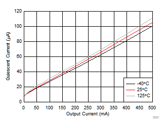
Figure 1. Quiescent Current vs Output Current
TPS7B68-Q1 D003_SLVSD43.gif
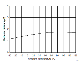
Figure 3. Shutdown Current vs Ambient Temperature
TPS7B68-Q1 D005_SLVSD43.gif
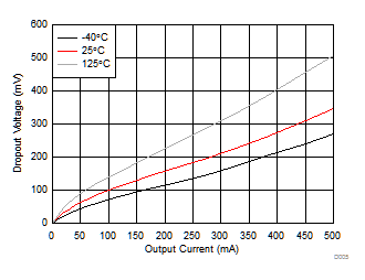
Figure 5. Dropout Voltage vs Output Current
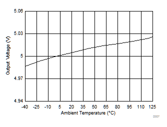
TPS7B68-Q1 D007_SLVSD43.gif
VOUT = 5 V
Figure 7. Output Voltage vs Ambient Temperature
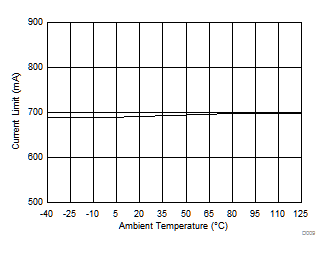
TPS7B68-Q1 D009_SLVSD43.gif
VIN = 5.6 V
Figure 9. Output Current Limit (ILIM) vs Ambient Temperature
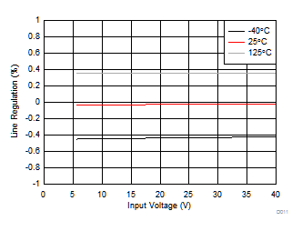
TPS7B68-Q1 D011_SLVSD43.gif
Figure 11. Line Regulation
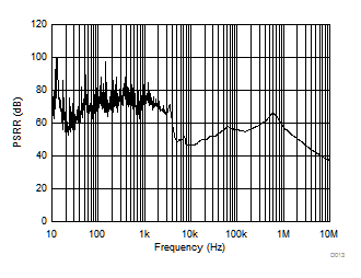
TPS7B68-Q1 D013_SLVSD43.gif
COUT = 10 μF IOUT = 100 mA TA = 25°C
Figure 13. PSRR vs Frequency
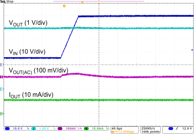
TPS7B68-Q1 D015_SLVSD43.gif
VIN = 6 V to 40 V VOUT = 5 V COUT = 10 µF
IOUT = 1 mA
Figure 15. Line Transient
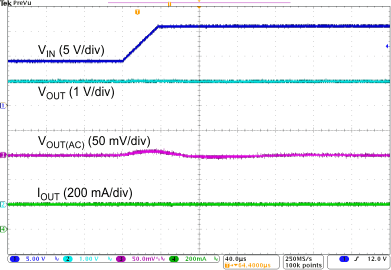
TPS7B68-Q1 D017_SLVSD43.gif
VIN = 6 V to 40 V VOUT = 5 V COUT = 10 µF
IOUT = 200 mA
Figure 17. Line Transient
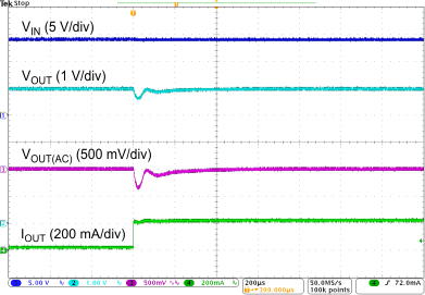
TPS7B68-Q1 D019_SLVSD43.gif
VOUT = 5 V COUT = 10 µF IOUT = 1 mA to 200 mA
Figure 19. Load Transient
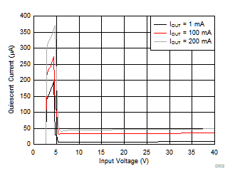
TPS7B68-Q1 D002_SLVSD43.gif
Figure 2. Quiescent Current vs Input Voltage
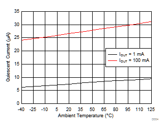
TPS7B68-Q1 D004_SLVSD43.gif
Figure 4. Quiescent Current vs Ambient Temperature
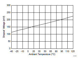
TPS7B68-Q1 D006_SLVSD43.gif
IOUT = 200 mA
Figure 6. Dropout Voltage vs Ambient Temperature
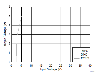
TPS7B68-Q1 D008_SLVSD43.gif
VOUT = 5 V
Figure 8. Output Voltage vs Input Voltage
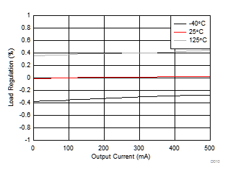
TPS7B68-Q1 D010_SLVSD43.gif
Figure 10. Load Regulation
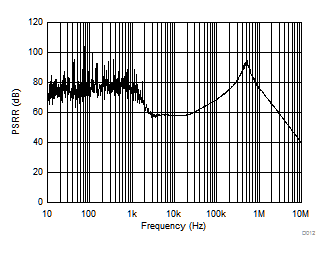
TPS7B68-Q1 D012_SLVSD43.gif
COUT = 10 μF IOUT = 1 mA TA = 25°C
Figure 12. PSRR vs Frequency
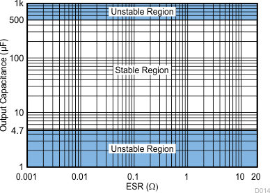
TPS7B68-Q1 D014A_SLVSD43.gif
Figure 14. ESR Stability vs Output Capacitance
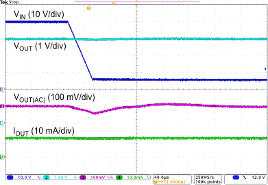
TPS7B68-Q1 D016_SLVSD43.gif
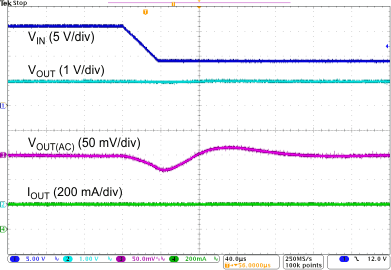
VIN = 40 V to 6 V VOUT = 5 V COUT = 10 µF
IOUT = 1 mA
Figure 16. Line Transient
TPS7B68-Q1 D018_SLVSD43.gif
VIN = 40 V to 6 V VOUT = 5 V COUT = 10 µF
IOUT = 200 mA
Figure 18. Line Transient
TPS7B68-Q1 D020_SLVSD43.gif
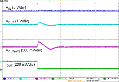
VOUT = 5 V COUT = 10 µF IOUT = 200 mA to 1 mA
Figure 20. Load Transient