SLVSDW6C April 2017 – April 2021 TPS7H1101A-SP
PRODUCTION DATA
- 1 Features
- 2 Applications
- 3 Description
- 4 Revision History
- 5 Pin Configuration and Functions
- 6 Specifications
- 7 Detailed Description
- 8 Application and Implementation
- 9 Power Supply Recommendations
- 10Layout
- 11Device and Documentation Support
- 12Mechanical, Packaging, and Orderable Information
Package Options
Mechanical Data (Package|Pins)
- HKR|16
- KGD|0
Thermal pad, mechanical data (Package|Pins)
Orderable Information
8.1.1 Stability
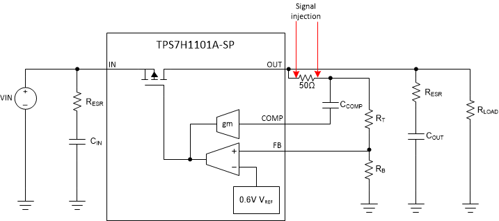
Bode plots are a standard approach in assessing stability. This approach requires a single feedback path where an AC signal is injected across a resistor (typically 50 Ω) and measurements are taken on either side of the resistor as shown in Figure 8-1. From this measurement, loop gain and phase plots can be generated. Crossover frequency, ƒC, is defined as the frequency where the magnitude of the loop gain is unity and phase margin is evaluated at the crossover frequency ƒC.
 Figure 8-1 Conventional Bode Plot With Simplified Feedback Loops
However, it is important the AC signal is injected as shown in Figure 8-1. This injection point ensures that the feedback signal goes through both the outer loop (consisting of the top feedback resistor, RT) and the inner loop (consisting of the compensation capacitor, CCOMP). If the only the outer loop is measured, the resulting crossover frequency will be lower which would indicate a poorer transient response than reality. Therefore, it is best to inject the measurement signal at a point where it goes through both loops. If this is not possible, the two loops may be measured independently and added using the superposition principle.
Furthermore, the stability of the device can be qualitatively validated by applying a step load to the output and observing the response. The SPICE models for the device can be found on the TPS7H1101A-SP product page. To simulate impedance measurements, the transient model should be used.