SLVSFT8F February 2023 – December 2023 TPS7H1111-SEP , TPS7H1111-SP
PRODUCTION DATA
- 1
- 1 Features
- 2 Applications
- 3 Description
- 4 Device Options Table
- 5 Pin Configuration and Functions
- 6 Specifications
- 7 Parameter Measurement Information
-
8 Detailed Description
- 8.1 Overview
- 8.2 Functional Block Diagram
- 8.3 Feature Description
- 8.4 Device Functional Modes
-
9 Application and Implementation
- 9.1 Application Information
- 9.2 Typical Applications
- 9.3 Capacitors Tested
- 9.4 TID Effects
- 9.5 Power Supply Recommendations
- 9.6 Layout
- 10Device and Documentation Support
- 11Revision History
- 12Mechanical, Packaging, and Orderable Information
Package Options
Refer to the PDF data sheet for device specific package drawings
Mechanical Data (Package|Pins)
- PWP|28
Thermal pad, mechanical data (Package|Pins)
- PWP|28
Orderable Information
8.3.2 Output Voltage Configuration
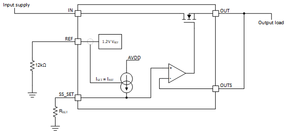
The output voltage of the TPS7H1111 is set by placing a resistor, RSET, from the SS_SET pin to GND. During nominal operation, 100 μA is output from the SS_SET pin. By appropriately selecting RSET, the desired output voltage will be generated on the SS_SET pin as calculated in Equation 1. This voltage will be replicated on the output through the internal unity gain error amplifier as shown in Figure 8-1.
where
- ISET = 100 μA (typ)
- VSS_SET = set voltage that is configured to the desired output voltage, VOUT
 Figure 8-1 Simplified Schematic to
Configure Output Voltage
Figure 8-1 Simplified Schematic to
Configure Output VoltageThe 100 μA reference current is configured by placing a 12 kΩ resistor from the REF pin to GND. The 1.2 V across the RREF resistor will create an approximate 100 μA reference current. This current is mirrored to the SS_SET pin to create a highly accurate reference current. Generally 0.1% precision resistors are recommended for RREF and RSET to precisely set the currents. If precision 0.1% resistors are utilized, the ISS_SET error due to the RREF resistor will be 0.1%. Additionally, the 0.1% error of the RSET resistor will also contribute to VOUT accuracy error. The TPS7H1111 accuracy specification is +1.2% / –1.3% across line, load, and temperature, but resistor tolerance error must be separately added. Common output voltages and resistor values are shown in Table 8-4.
| Output Voltage, VOUT | Value for 0.1% Tolerance Resistors |
|---|---|
| 0.4 V | 4.02 kΩ |
| 0.7 V | 6.98 kΩ |
| 1 V | 10 kΩ |
| 1.1 V | 11 kΩ |
| 1.2 V | 12 kΩ |
| 1.5 V | 15 kΩ |
| 1.8 V | 18 kΩ |
| 2.5 V | 24.9 kΩ |
| 3.3 V | 33.2 kΩ |
| 4 V | 40.2 kΩ |
| 5 V | 49.9 kΩ |
Additionally, if greater accuracy is desired, matched resistors may be utilized (which are often available in accuracy ratios better than 0.1%). For example, a nominal 12 kΩ ± 5% resistor could be selected for RREF with a matched resistor so that the that RSET / RREF ratio is 0.01% (or even better). In this case, instead of Equation 1 to calculate the set voltage, use Equation 2.
where
- VSS_SET = set voltage that is set to the desired output voltage, VOUT
Equation 2 allows one to easily calculate errors in the set output voltage due to RREF and RSET resistor mismatch. However, while improved resistor ratios will likely improve the output accuracy, other error sources are still present. These sources include the inherent reference current accuracy itself and error amplifier offset voltage.
The output voltage accuracy, VACC, specifies a minimum accuracy of –1.3% and maximum accuracy of +1.2% in the Electrical Characteristics table. This specification applies across the complete temperature range of –55°C to 125°C, across all the input voltages (0.85 V ≤ VIN ≤ 7 V and 2.2 V ≤ VBIAS ≤ 14 V), and up to full load (1 mA ≤ IOUT ≤ 1.5 A). A few additional details to the measurement are noted:
- The range of VIN, VBIAS, IOUT, and temperature mean the specification applies across all line, load, and temperature combinations. This is accomplished by testing multiple bias conditions that cover various corners.
- Footnote 4 in the Electrical Characteristics specifies VBIAS ≥ VIN and VBIAS ≥ VOUT + 1.6 V. This is because not all extreme corners of VIN and VBIAS are feasible (for example, VIN = 7 V and VBIAS = 2.2 V would not make sense).
- Footnote 5 in the Electrical Characteristics specifies that the measurement is done with a power dissipation that is limited to a maximum of 4 W. This is due to tester thermal limitations. On a typical application board with good thermals, there is no inherent limitation.
- The test conditions specify a minimum of 1 mA and not 0 mA for more robust accuracy measurements. However, in a normal application the TPS7H1111 device does not have a minimum load current for stability.
- The post TID specification is measured at room temperature (a MIL standard in order to avoid annealing at high temperatures). The TPS7H1111 is specified post TID to have a minimum accuracy of –0.7% and maximum of +1.1%. This is compared to a pre-TID accuracy of –0.7% and maximum of +0.9%.
- TI does not recommend including the following error terms into the VACC specification as they are inherently covered in the VACC parameter itself: ISET current accuracy, VOS (output offset voltage), VREF voltage accuracy, ΔVOUT/ΔVIN (line regulation), ΔVOUT/ΔIOUT (load regulation), or VOUTtempco.
- The error due to external components, such as RREF and RSET resistor tolerances, may be added to VACC specifications as this is not included in the parameter.
For additional information on determining output voltage accuracy, see Section 9.2.1.2.3.