SLVSFT8F February   2023  – December 2023 TPS7H1111-SEP , TPS7H1111-SP

PRODUCTION DATA  

  1.   1
  2. Features
  3. Applications
  4. Description
  5. Device Options Table
  6. Pin Configuration and Functions
  7. Specifications
    1. 6.1 Absolute Maximum Ratings
    2. 6.2 ESD Ratings
    3. 6.3 Recommended Operating Conditions
    4. 6.4 Thermal Information
    5. 6.5 Electrical Characteristics
    6. 6.6 Quality Conformance Inspection
    7. 6.7 Typical Characteristics
  8. Parameter Measurement Information
  9. Detailed Description
    1. 8.1 Overview
    2. 8.2 Functional Block Diagram
    3. 8.3 Feature Description
      1. 8.3.1  Bias Supply
      2. 8.3.2  Output Voltage Configuration
      3. 8.3.3  Output Voltage Configuration with a Voltage Source
      4. 8.3.4  Enable
      5. 8.3.5  Soft Start and Noise Reduction
      6. 8.3.6  Configurable Power Good
      7. 8.3.7  Current Limit
      8. 8.3.8  Stability
        1. 8.3.8.1 Output Capacitance
        2. 8.3.8.2 Compensation
      9. 8.3.9  Current Sharing
      10. 8.3.10 PSRR
      11. 8.3.11 Noise
      12. 8.3.12 Thermal Shutdown
    4. 8.4 Device Functional Modes
  10. Application and Implementation
    1. 9.1 Application Information
    2. 9.2 Typical Applications
      1. 9.2.1 Application 1: Set Turn-On Threshold with EN
        1. 9.2.1.1 Design Requirements
        2. 9.2.1.2 Detailed Design Procedure
          1. 9.2.1.2.1 Bias Supply
          2. 9.2.1.2.2 Output Voltage Configuration
          3. 9.2.1.2.3 Output Voltage Accuracy
          4. 9.2.1.2.4 Enable Threshold
          5. 9.2.1.2.5 Soft Start and Noise Reduction
          6. 9.2.1.2.6 Configurable Power Good
          7. 9.2.1.2.7 Current Limit
          8. 9.2.1.2.8 Output Capacitor and Ferrite Bead
        3. 9.2.1.3 Application Curve
      2. 9.2.2 Application 2: Parallel Operation
        1. 9.2.2.1 Design Requirements
        2. 9.2.2.2 Detailed Design Procedure
          1. 9.2.2.2.1 Current Sharing
        3. 9.2.2.3 Application Results
    3. 9.3 Capacitors Tested
    4. 9.4 TID Effects
    5. 9.5 Power Supply Recommendations
    6. 9.6 Layout
      1. 9.6.1 Layout Guidelines
      2. 9.6.2 Layout Example
  11. 10Device and Documentation Support
    1. 10.1 Documentation Support
      1. 10.1.1 Third-Party Products Disclaimer
      2. 10.1.2 Related Documentation
    2. 10.2 Receiving Notification of Documentation Updates
    3. 10.3 Support Resources
    4. 10.4 Trademarks
    5. 10.5 Electrostatic Discharge Caution
    6. 10.6 Glossary
  12. 11Revision History
  13. 12Mechanical, Packaging, and Orderable Information

Package Options

Refer to the PDF data sheet for device specific package drawings

Mechanical Data (Package|Pins)
  • HBL|14
  • PWP|28
Thermal pad, mechanical data (Package|Pins)
Orderable Information

Parameter Measurement Information

GUID-20200813-CA0I-SH51-XGJT-M8V5TN2GRSKK-low.png
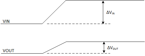
ΔVOUT / ΔVIN = 3 µV/V (typ). This means for a 1 V change in VIN (ΔVIN = 1 V), there will be a 3 µV change in VOUT (ΔVOUT = 3 µV). Line regulation is a DC parameter; therefore this waveform should only be considered valid after transients die out or for a slow VIN slew rate.
Figure 7-1 Line Regulation
GUID-20200813-CA0I-M2NC-FRVX-VQG53FXBGBHZ-low.png
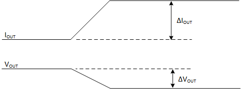
ΔVOUT / ΔIOUT = 500 µV/A (typ). This means for a 1 A change in IOUT (ΔIOUT = 1 A), there will be a 500 µV change in VOUT (ΔVOUT = 500 µV). Load regulation is a DC parameter; therefore this waveform should only be considered valid after transients die out or for a slow IOUT slew rate.
Figure 7-2 Load Regulation