SLVSFT8F February 2023 – December 2023 TPS7H1111-SEP , TPS7H1111-SP
PRODUCTION DATA
- 1
- 1 Features
- 2 Applications
- 3 Description
- 4 Device Options Table
- 5 Pin Configuration and Functions
- 6 Specifications
- 7 Parameter Measurement Information
-
8 Detailed Description
- 8.1 Overview
- 8.2 Functional Block Diagram
- 8.3 Feature Description
- 8.4 Device Functional Modes
-
9 Application and Implementation
- 9.1 Application Information
- 9.2 Typical Applications
- 9.3 Capacitors Tested
- 9.4 TID Effects
- 9.5 Power Supply Recommendations
- 9.6 Layout
- 10Device and Documentation Support
- 11Revision History
- 12Mechanical, Packaging, and Orderable Information
Package Options
Refer to the PDF data sheet for device specific package drawings
Mechanical Data (Package|Pins)
- HBL|14
- PWP|28
Thermal pad, mechanical data (Package|Pins)
- PWP|28
Orderable Information
3 Description
The TPS7H1111 is an ultra-low noise, high PSRR, low dropout linear regulator (LDO) optimized for powering radio-frequency (RF) devices in a space environment. It is capable of sourcing up to 1.5 A over a 0.85-V to 7-V input range with a 2.2-V to 14-V bias supply.
The high performance of the device limits power-supply generated phase noise and clock jitter, making this device ideal for powering high-performance ADCs, DACs, VCOs, PLLs, SerDes, and other RF components in satellites. For digital loads (such as FPGAs and DSPs) requiring low voltage operation, the exceptional accuracy and excellent transient performance ensure optimal system performance.
A standard microcircuit drawing (SMD) is available for the QML variants, 5962R21203. A vendor item drawing (VID) is available for the -SEP variant, V62/23602.
| PART NUMBER(1) | GRADE | PACKAGE(2) |
|---|---|---|
| 5962R2120301VXC | QMLV-RHA | 14-pin ceramic8.03 mm × 9.12 mmMass = 1.23 g |
| TPS7H1111HBL/EM | Engineering sample | |
| 5962R2120302PYE | QMLP-RHA | 28-pin plastic 4.40 mm × 9.70 mm Mass = 198 mg |
| TPS7H1111MPWPTSEP | SEP |
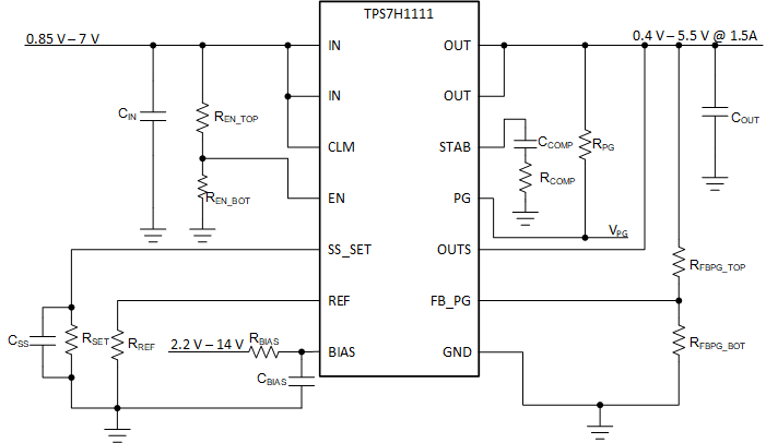
 Typical
Application Circuit