SLVSAS4J June 2013 – April 2017 TPS7H1201-HT
PRODUCTION DATA.
- 1 Features
- 2 Applications
- 3 Description
- 4 Revision History
- 5 Pin Configuration and Functions
- 6 Specifications
- 7 Detailed Description
- 8 Application and Implementation
- 9 Power Supply Recommendations
- 10Layout
- 11Device and Documentation Support
- 12Mechanical, Packaging, and Orderable Information
Package Options
Mechanical Data (Package|Pins)
- HKS|16
- KGD|0
Thermal pad, mechanical data (Package|Pins)
Orderable Information
8 Application and Implementation
NOTE
Information in the following applications sections is not part of the TI component specification, and TI does not warrant its accuracy or completeness. TI’s customers are responsible for determining suitability of components for their purposes. Customers should validate and test their design implementation to confirm system functionality.
8.1 Application Information
The TPS7H1201-HT LDO linear regulator is targeted to harsh environment applications. This regulator has various features such as low dropout, soft start, output current foldback, high-side current sensing (where sensing voltage at CS pin provides voltage proportional to output current), and current sharing.
8.1.1 Stability
Conventional Bode plots are a standard approach in assessing stability as shown in Figure 13. This approach requires that we have a single feedback path where an AC signal is injected across a resistor (typically 50 Ω) and measurements are taken on either side of the resistor. From this, loop gain and phase plots can be generated. Crossover frequency, ƒC, is defined as the frequency where the magnitude of the loop gain is unity and phase margin is evaluated at the crossover frequency ƒC.
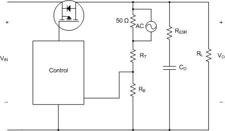 Figure 13. Conventional Bode Plot
However, there are conditions where the feedback loop is not accessible or there may be multiple feedback paths, as with the TPS7H1101-SP. When there are multiple feedback loops the conventional bode plot approach will not be representative of the device's true response. The TPS7H1101-SP uses a conventional feedback loop in addition to an inner fast loop that injects current into the error amplifier, which in turn greatly improves the transient response of the device. The Bode plot method can still be used to understand the behavior of the main loop, but this will show a lower crossover frequency and thus imply a slower transient response than the actual performance of the device. Fortunately, accurate and quantitative stability metrics can still be assessed from output impedance measurements and simulations.
There are multiple ways output impedance can be measured. One approach is to inject a small current at the output of the regulator and compare it to the resulting voltage response. The variation in the phase of the output impedance across frequency can be related to the phase margin through the group delay.
Group delay, Tg, is the rate of change of phase with respect to frequency as shown in Equation 2. Most SPICE simulation packages can plot this parameter and certain frequency analyzers boast software that supports a direct measurement. Using this software, phase margin can be extracted from the group delay plot. The phase margin and crossover frequency reported from these measurements will include the effects of both feedback loops.
The stability of the device can be qualitatively validated by applying a step load to the output and observing the response. The SPICE models for the device can be found in Tools & Software on the product page. To simulate impedance measurements, the transient model should be used. For a more detailed explanation of this approach and how to use the model to simulate the output impedance and group delay, please see reference (1).
8.2 Typical Application
8.2.1 Design Requirements
Table 1 shows the design parameters.
Table 1. Design Parameters
| PARAMETER | VALUE | |||
|---|---|---|---|---|
| Input voltage | 1.5 V to 7 V | |||
| Output voltage | User programmable | |||
| Output current | 3-A max | |||
8.2.2 Detailed Design Procedure
8.2.2.1 Adjustable Output Voltage (Feedback Circuit)
The output voltage of the TPS7H1201-HT can be set to a user-programmable level between 0.8 and 6.8 V. Achieve this by using a resistor divider connected between VOUT, FB, and GND terminals. RTOP connected between VOUT and VFB, and RBOTTOM connected between VFB and GND.
Use Equation 3 to determine VOUT.

where
- VFB = 0.605 V
Table 2. Resistor Values for Typical Voltages
| VOUT | Standard 1% Resistors | Standard 0.1% Resistors | ||
|---|---|---|---|---|
| RTOP | RBOTTOM | RTOP | RBOTTOM | |
| 0.8 V | 10.7 kΩ | 33.2 kΩ | 10.7 kΩ | 33.2 kΩ |
| 1 V | 13.7 kΩ | 21 kΩ | 12.6 kΩ | 19.3 kΩ |
| 1.2 V | 11.3 kΩ | 11.5 kΩ | 11.8 kΩ | 12 kΩ |
| 1.5 V | 15.8 kΩ | 10.7 kΩ | 18.2 kΩ | 12.3 kΩ |
| 1.8 V | 23.2 kΩ | 11.8 kΩ | 32 kΩ | 16.2 kΩ |
| 2.5 V | 10.7 kΩ | 3.4 kΩ | 37.9 kΩ | 12.1 kΩ |
| 3.3 V | 51.1 kΩ | 11.5 kΩ | 10.2 kΩ | 2.29 kΩ |
| 4 V | 13.3 kΩ | 2.37 kΩ | 31.2 kΩ | 5.56 kΩ |
| 5 V | 11.5 kΩ | 1.58 kΩ | 16.2 kΩ | 2.23 kΩ |
| 5.5 V | 17.4 kΩ | 2.15 kΩ | 89.8 kΩ | 11.1 kΩ |
| 6 V | 90.9 kΩ | 10.2 kΩ | 10.7 kΩ | 1.2 kΩ |
| 6.5 V | 26.7 kΩ | 2.74 kΩ | 15.2 kΩ | 1.56 kΩ |
| 6.6 V | 11.3 kΩ | 1.15 kΩ | 22.1 kΩ | 2.23 kΩ |
| 6.7 V | 39.2 kΩ | 3.92 kΩ | 13.8 kΩ | 1.37 kΩ |
8.2.2.2 PCL
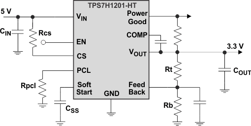
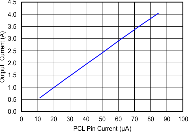
PCL resistor, Rpcl, sets the overcurrent limit activation point and can be calculated per Equation 4.
where
- Vref = 0.605 V
- ICL = Programmable current limit (A)
- Current sense ratio (CSR) is the ratio of output load current to ICS. The typical value of the CSR is 47394.
Figure 15 shows the output load current (IOUT) versus PCL terminal current (ICL)
A suitable resistor Rpcl must be chosen to ensure the CS terminal is within its operating range of 0.3 V to VIN.
The maximum PCL is 700 mA. The range of resistor that can be used on the PCL terminal to GND is 47 kΩ to 160 kΩ.
8.2.2.3 High-Side Current Sense
Figure 16 shows the cascode NMOS current mirror. Vcs must be in the range as specified in the Electrical Characteristics table. The following example shows the typical calculation of Rcs.


where
- ILOAD is the output load current.
- CSR is the current sense ratio.
When VIN = 2.3 V, select VCS = 2.05 V, ILOAD = 3 A, CSR = 47394, and Ioffset = 0.1899 A, then ICS = 67.306 µA and RCS = 3.714 kΩ.
 Figure 16. Cascode NMOS Current Mirror
For TPS7H1201-HT, Figure 17 shows the typical curve VCS vs IOUT for VIN = 2.28 V and RCS = 3.65 kΩ. A resistor connected from the CS terminal to VIN indicates voltage proportional to the output current.
Monitoring current in the CS terminal (ICS vs IOUT) indicates the current sense ratio between the main PMOSFET and the current sense MOSFET as shown in .
Figure 19 shows IOUT vs ICS when the voltage on CS terminal is varied from 0.3 V to 7 V.
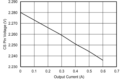
| y = –0.0732x + 2.2804 | |||
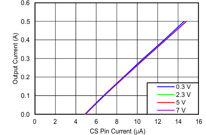
| VIN = 2.3 V | VOUT = 1.8 V |

| y = 49917x – 0.2466 | |||
8.2.2.4 Current Foldback
- The TPS7H1201-HT has a current foldback feature which can be enabled when the CS terminal is held high. Shorting CS low disables the foldback current limit. If the foldback current limit is disabled, then the LDO will begin regulating again as soon as the current falls below the clamp threshold.
- With foldback current limit enabled, when current limit trip point is activated,
- Output voltage drops low.
- Output current folds back to approximately 50% of the current limit trip point.
8.2.2.5 Transient Response
Figure 20, Figure 21, and Figure 22 indicate the transient response behavior of the TPS7H1201-HT.
Channel 1: Output voltage overshoot/undershoot
Channel 2: Step load in current
Channel 3: Input voltage
 Figure 20. Load Transient Response: Step Load 0 A to
 250 µA, VIN = 2.3 V, VOUT = 1.8 V
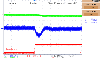 Figure 22. Expanded View Undershoot
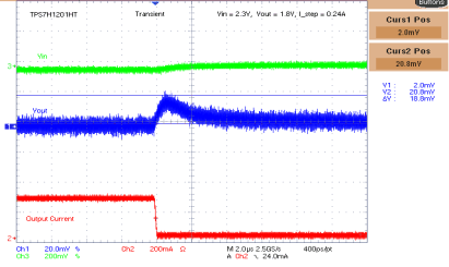 Figure 21. Expanded View Overshoot
8.2.2.6 Current Sharing
For demanding load requirements, multiple LDOs can be paralleled as indicated in Figure 24. In parallel mode, the CS terminal of LDO1 must be connected to the PCL terminal of LDO2 via a series resistor RCL, and CS terminal of LDO2 must be connected to PCL terminal of LDO1 via series resistor RCL. The typical value of RCL in parallel operation is 3.75 kΩ for current limit > 6 A. In parallel configuration, RCL (resistor from PCL to GND) and RCS (resistor from CS terminal to VIN) must be left open (unpopulated). The RCL value must be selected so that the operating condition of the CS terminal is maintained, as specified in the Electrical Characteristics table. The current from PCL through RCL of LDO1 is determined by the output load current of LDO2 divided by the CSR. Hence, the voltage at CS terminal of the LDO1 is 0.605 V – ((output load current of LDO2 + 0.2458) / CSR × RCL).
Alternately, it can also provide twice the output current to meet system needs. When using two LDOs in parallel operation for higher output load current, use POL TPS50601-SP as an input source.

 Figure 24. Block Diagram (Parallel Operation)
8.2.2.7 Compensation
Figure 25 shows a generic block diagram for TPS7H1201-HT LDO with external compensation components. LDO incorporates nested loops, thus providing the high gain necessary to meet design performance.
 Figure 25. TPS7H1201-HT Compensation
Resistor divider composed of Rtop and Rbottom determine the output voltage set points as indicated by Equation 3.
Output capacitor COUT introduces a pole and a zero as shown in the following.


The TPS7H1101-SP was designed so that the ESR of the output capacitor will not have a strong influence on the response of the LDO. However, an optional capacitor, Cx, can be added in parallel with the bottom feedback resistor to introduce a pole to cancel Fz_co. Equation 9 shows how to calculate the location of the pole introduced by Cx. To cancel the zero directly, Fp should be equal to Fz_co.

Cx is calculated to be 1000 pF for Co = 220 µF, Cesr = 45 mΩ, and Rbottom = 10 kΩ.
Internal compensation in the LDO cancels the output capacitor pole introduced by COUT and RL.
Ccomp introduces a dominant pole at low frequency. TI recommends that a Ccomp value of 10 nF.
8.2.2.8 Output Noise
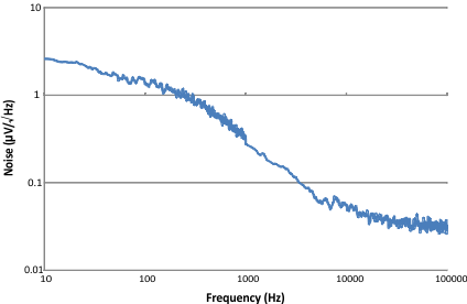
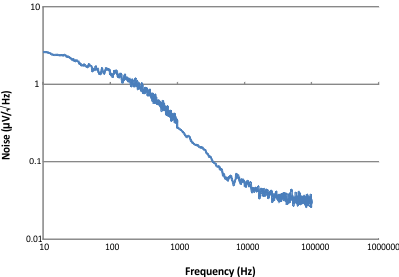
Output noise is measured using an HP3495A. , , Figure 26, and Figure 27 show noise of the TPS7H1201-HT in µV/√Hz vs frequency.
8.2.2.9 Capacitors
TPS7H1201-HT requires the use of a combination of tantalum and ceramic capacitors to achieve good volume to capacitance ratio. Table 3 highlights some of the capacitors used in the device. TI recommends to follow proper derating guidelines as recommended by the capacitor manufacturer based upon output voltage and operating temperature.
Note that polymer-based tantalum capacitors must be derated to at least 60% of rated voltage, whereas manganese oxide (MnO2) based tantalum capacitors should be derated to 33% of rated voltage depending upon the operating temperature.
TI recommends to use a tantalum capacitor along with a 0.1-µF ceramic capacitor. The device is stable for input and output tantalum capacitor values of 10 to 220 µF with the ESR range of 10 mΩ to 2 Ω. However, the dynamic performance of the device varies based on load conditions and the capacitor values used.
TI recommends a minimum output capacitor of 22 µF with ESR of 1 Ω or less to prevent oscillations. X7R dielectrics are preferred. See Table 3 for various capacitor recommendations.
Table 3. TPS7H1201-HT Capacitors
| CAPACITOR PART NUMBER | CAPACITOR DETAILS (CAPACITOR, VOLTAGE, ESR) |
TYPE | VENDOR |
|---|---|---|---|
| T493X107K016CH612A(1) | 100 µF, 16 V, 100 mΩ | Tantalum - MnO2 | Kemet |
| T493X226M025AH6x20(1) | 22 µF, 25 V, 35 mΩ | Tantalum - MnO2 | Kemet |
| T525D476M016ATE035(1) | 47 µF, 10 V, 35 mΩ | Tantalum - Polymer | Kemet |
| T540D476M016AH6520(1) | 47 µF, 16 V, 20 mΩ | Tantalum - Polymer | Kemet |
| T525D107M010ATE025(1) | 100 µF, 10 V, 25 mΩ | Tantalum - Polymer | Kemet |
| T541X337M010AH6720(1) | 330 µF, 10 V, 6 mΩ | Tantalum - Polymer | Kemet |
| T525D227M010ATE025(1) | 220 µF, 10 V, 25 mΩ | Tantalum - Polymer | Kemet |
| T495X107K016ATE100(1) | 100 µF, 16 V, 100 mΩ | Tantalum - MnO2 | Kemet |
| CWR29FK227JTHC(1) | 220 µF, 10 V, 180 mΩ | Tantalum - MnO2 | AVX |
| THJE107K016AJH | 100 µF, 16 V, 58 mΩ | Tantalum | AVX |
| THJE227K010AJH | 220 µF, 10 V, 40 mΩ | Tantalum | AVX |
| SMX33C336KAN360 | 33 µF, 25 V | Stacked ceramic | AVX |
| SR2225X7R335K1P5#M123 | 3.3 µF, 25 V, 10 mΩ | Ceramic | Presidio Components Inc |
8.2.3 Application Curves
 Figure 28. VDO vs IOUT
 Figure 29. LDO Current Share

