SLVSGG1A February 2022 – September 2022 TPS7H5005-SEP , TPS7H5006-SEP , TPS7H5007-SEP , TPS7H5008-SEP
PRODUCTION DATA
- 1 Features
- 2 Applications
- 3 Description
- 4 Revision History
- 5 Device Comparison Table
- 6 Pin Configuration and Functions
-
7 Specifications
- 7.1 Absolute Maximum Ratings
- 7.2 ESD Ratings
- 7.3 Recommended Operating Conditions
- 7.4 Thermal Information
- 7.5 Electrical Characteristics: All Devices
- 7.6 Electrical Characteristics: TPS7H5005-SEP
- 7.7 Electrical Characteristics: TPS7H5006-SEP
- 7.8 Electrical Characteristics: TPS7H5007-SEP
- 7.9 Electrical Characteristics: TPS7H5008-SEP
- 7.10 Typical Characteristics
-
8 Detailed Description
- 8.1 Overview
- 8.2 Functional Block Diagram
- 8.3
Feature Description
- 8.3.1 VIN and VLDO
- 8.3.2 Start-Up
- 8.3.3 Enable and Undervoltage Lockout (UVLO)
- 8.3.4 Voltage Reference
- 8.3.5 Error Amplifier
- 8.3.6 Output Voltage Programming
- 8.3.7 Soft Start (SS)
- 8.3.8 Switching Frequency and External Synchronization
- 8.3.9 Primary Switching Outputs (OUTA/OUTB)
- 8.3.10 Synchronous Rectifier Outputs (SRA/SRB)
- 8.3.11 Dead Time and Leading Edge Blank Time Programmability (PS, SP, and LEB)
- 8.3.12 Pulse Skipping
- 8.3.13 Duty Cycle Programmability
- 8.3.14 Current Sense and PWM Generation (CS_ILIM)
- 8.3.15 Hiccup Mode Operation (HICC)
- 8.3.16 External Fault Protection (FAULT)
- 8.3.17 Slope Compensation (RSC)
- 8.3.18 Frequency Compensation
- 8.3.19 Thermal Shutdown
- 8.4 Device Functional Modes
-
9 Application and Implementation
- 9.1 Application Information
- 9.2
Typical Application
- 9.2.1 Design Requirements
- 9.2.2
Detailed Design Procedure
- 9.2.2.1 Switching Frequency
- 9.2.2.2 Output Voltage Programming Resistors
- 9.2.2.3 Dead Time
- 9.2.2.4 Leading Edge Blank Time
- 9.2.2.5 Soft-Start Capacitor
- 9.2.2.6 Transformer
- 9.2.2.7 Main Switching FETs
- 9.2.2.8 Synchronous Rectificier FETs
- 9.2.2.9 RCD Clamp
- 9.2.2.10 Output Inductor
- 9.2.2.11 Output Capacitance and Filter
- 9.2.2.12 Sense Resistor
- 9.2.2.13 Hiccup Capacitor
- 9.2.2.14 Frequency Compensation Components
- 9.2.2.15 Slope Compensation Resistor
- 10Power Supply Recommendations
- 11Layout
- 12Device and Documentation Support
- 13Mechanical, Packaging, and Orderable Information
Package Options
Mechanical Data (Package|Pins)
- PW|24
Thermal pad, mechanical data (Package|Pins)
Orderable Information
8.3.14 Current Sense and PWM Generation (CS_ILIM)
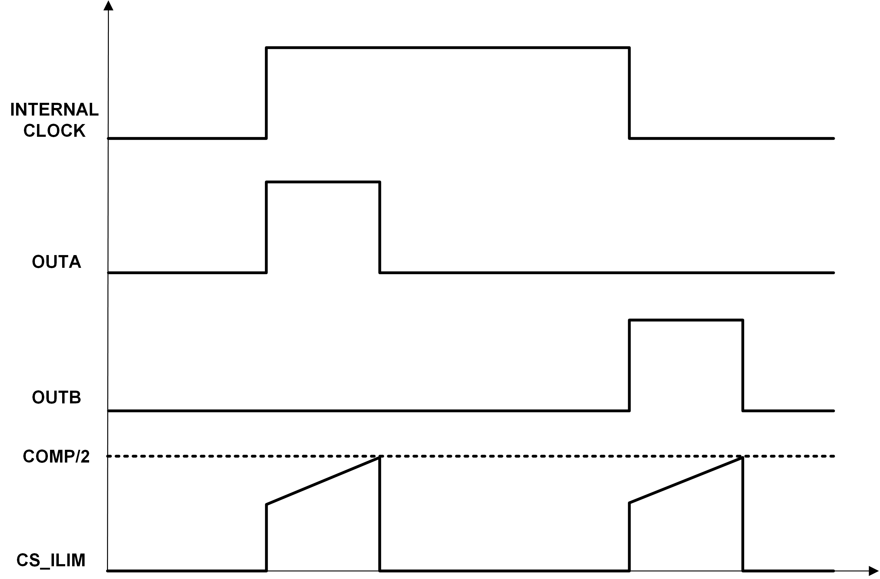
The CS_ILIM pin is driven by a signal representative of the transformer primary-side current. The current signal has to have compatible input range of the COMP pin. As shown in Figure 8-14, the COMP pin voltage is used as the reference for the peak current. Note that the OUTB waveform is only applicable for TPS7H5005-SEP and TPS7H5008-SEP. The primary side signals, OUTA/OUTB, are turned on by the internal clock signal and turned off when sensed peak current reaches the COMP/2 pin voltage. Note that this peak sensed current signal that is compared to COMP/2 at the PWM comparator contains an offset voltage of 150 mV. The CS_ILIM pin is also used to configure the current limit for the controller.
 Figure 8-14 Peak Current Mode Control and
PWM Generation
Figure 8-14 Peak Current Mode Control and
PWM GenerationA resistor is needed from CS_ILIM to AVSS is used to detect current for both proper PWM operation and overcurrent protection. The current limit threshold VCS_ILIM, is specified as 1.05 V (nominal) in the electrical specifications. This indicates that when the voltage on this pin reaches this threshold, the device will go into hiccup mode. Equation 10 shows the calculation for determining the value of the sense resistor for a selected current limit.
Note that the value of ILIM has to account for where and how the current is being sensed. For a forward converter with sense resistor between source of primary FET to AVSS, ILIM will be referred to the primary side of the converter.
Equation 11 shows the calculation for determining ILIM in the design of a forward converter, where:
- IL,PEAK is the peak output inductor current desired to activate the overcurrent protection
- NS is the number of secondary turns for the power transformer
- NP is the number of primary turns for the power transformer
In the design of a buck converter which senses the high side current via a current sense transformer, Equation 12 can be used for determining ILIM for this instance.
In this equation:
- IL,PEAK is the peak output inductor current desired to activate the overcurrent protection
- NCSP is the number of primary turns of the current sense transformer
- NCSS is the number of secondary turns of the current sense transformer
Regardless of the topology, the user should ensure that there is sufficient margin between the peak current during normal operation and the overcurrent trip point when determining the value of RCS.