SNVSBZ6 May   2021 TPS92380 , TPS92381

PRODUCTION DATA  

  1. Features
  2. Applications
  3. Description
  4. Revision History
  5. Device Comparison Table
  6. Pin Configuration and Functions
  7. Specifications
    1. 7.1  Absolute Maximum Ratings
    2. 7.2  ESD Ratings
    3. 7.3  Recommended Operating Conditions
    4. 7.4  Thermal Information
    5. 7.5  Electrical Characteristics
    6. 7.6  Internal LDO Electrical Characteristics
    7. 7.7  Protection Electrical Characteristics
    8. 7.8  Current Sinks Electrical Characteristics
    9. 7.9  PWM Brightness Control Electrical Characteristics
    10. 7.10 Boost and SEPIC Converter Characteristics
    11. 7.11 Logic Interface Characteristics
    12. 7.12 Typical Characteristics
  8. Detailed Description
    1. 8.1 Overview
    2. 8.2 Functional Block Diagram
    3. 8.3 Feature Description
      1. 8.3.1 Integrated DC-DC Converter
        1. 8.3.1.1 DC-DC Converter Parameter Configuration
          1. 8.3.1.1.1 Switching Frequency
          2. 8.3.1.1.2 Spread Spectrum and External SYNC
          3. 8.3.1.1.3 Recommended Component Value and Internal Parameters
          4. 8.3.1.1.4 DC-DC Converter Switching Current Limit
          5. 8.3.1.1.5 DC-DC Converter Light Load Mode
        2. 8.3.1.2 Adaptive Voltage Control
          1. 8.3.1.2.1 Using Two-Divider
          2. 8.3.1.2.2 Using T-Divider
          3. 8.3.1.2.3 External Compensation
      2. 8.3.2 Internal LDO
      3. 8.3.3 LED Current Sinks
        1. 8.3.3.1 LED Output Configuration
        2. 8.3.3.2 LED Current Setting
        3. 8.3.3.3 Brightness Control
      4. 8.3.4 Fault Detections and Protection
        1. 8.3.4.1 Supply Fault and Protection
          1. 8.3.4.1.1 VIN Undervoltage Fault (VIN_UVLO)
          2. 8.3.4.1.2 VIN Overvoltage Fault (VIN_OVP)
        2. 8.3.4.2 Boost Fault and Protection
          1. 8.3.4.2.1 Boost Overvoltage Fault (BST_OVP)
          2. 8.3.4.2.2 SW Overvoltage Fault (SW_OVP)
        3. 8.3.4.3 LED Fault and Protection (LED_OPEN and LED_SHORT)
        4. 8.3.4.4 Thermal Fault and Protection (TSD)
        5. 8.3.4.5 Overview of the Fault and Protection Schemes
    4. 8.4 Device Functional Modes
      1. 8.4.1 STANDBY State
      2. 8.4.2 SOFT START State
      3. 8.4.3 BOOST START State
      4. 8.4.4 NORMAL State
      5. 8.4.5 FAULT RECOVERY State
      6. 8.4.6 State Diagram and Timing Diagram for Start-up and Shutdown
  9. Application and Implementation
    1. 9.1 Application Information
    2. 9.2 Typical Applications
      1. 9.2.1 Typical Application for 4 LED Strings
      2. 9.2.2 Design Requirements
      3. 9.2.3 Detailed Design Procedure
        1. 9.2.3.1 Inductor Selection
        2. 9.2.3.2 Output Capacitor Selection
        3. 9.2.3.3 Input Capacitor Selection
        4. 9.2.3.4 LDO Output Capacitor
        5. 9.2.3.5 Diode
      4. 9.2.4 Application Curves
      5. 9.2.5 SEPIC Mode Application
        1. 9.2.5.1 Design Requirements
        2. 9.2.5.2 Detailed Design Procedure
          1. 9.2.5.2.1 Inductor
          2. 9.2.5.2.2 Diode
          3. 9.2.5.2.3 Capacitor C1
        3. 9.2.5.3 Application Curves
  10. 10Power Supply Recommendations
  11. 11Layout
    1. 11.1 Layout Guidelines
    2. 11.2 Layout Example
  12. 12Device and Documentation Support
    1. 12.1 Device Support
      1. 12.1.1 Development Support
    2. 12.2 Documentation Support
      1. 12.2.1 Related Documentation
    3. 12.3 Receiving Notification of Documentation Updates
    4. 12.4 Support Resources
    5. 12.5 Trademarks
    6. 12.6 Electrostatic Discharge Caution
    7. 12.7 Glossary
  13. 13Mechanical, Packaging, and Orderable Information

Package Options

Mechanical Data (Package|Pins)
Thermal pad, mechanical data (Package|Pins)
Orderable Information

SEPIC Mode Application

When LED string voltage can be above or below VIN voltage, SEPIC configuration can be used. In this example, two separate coils or coupled coil could both be used for SEPIC. Separate coils can enable lower height external components to be used, compared to a coupled coil solution. On the other hand, coupled coil typically maximizes the efficiency. Also, in this example, an external clock is used to synchronize SEPIC switching frequency. External clock input can be modulated to spread switching frequency spectrum.
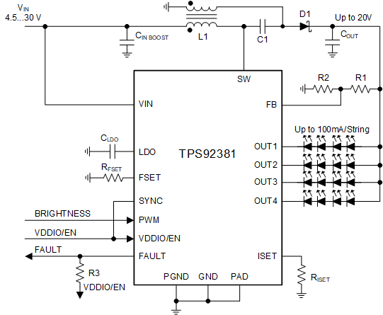
GUID-20210415-CA0I-6GSQ-5LFC-VQGXCX9JDW91-low.gif Figure 9-4 SEPIC Mode, 4 Strings 100 mA per String Configuration