SLUSDG2 October 2018 TPS92515AHV-Q1
PRODUCTION DATA.
- 1 Features
- 2 Applications
- 3 Description
- 4 Revision History
- 5 Device Comparison Table
- 6 Pin Configuration and Functions
- 7 Specifications
-
8 Detailed Description
- 8.1 Overview
- 8.2 Functional Block Diagram
- 8.3
Feature Description
- 8.3.1 General Operation
- 8.3.2 Current Sense Comparator
- 8.3.3 OFF Timer
- 8.3.4 OFF-Timer, Shunt FET Dimming or Shunted Output Condition
- 8.3.5 Internal N-channel MOSFET
- 8.3.6 VCC Internal Regulator and Undervoltage Lockout (UVLO)
- 8.3.7 Analog Adjust Input
- 8.3.8 Thermal Protection
- 8.3.9 Junction Temperature Relative Estimation
- 8.3.10 BOOT and BOOT UVLO
- 8.3.11 PWM (UVLO and Enable)
- 8.4 Device Functional Modes
-
9 Application and Implementation
- 9.1 Application Information
- 9.2
Typical Application
- 9.2.1 General Design Procedure
- 9.2.2 Design Requirements
- 9.2.3
Detailed Design Procedure
- 9.2.3.1 Calculating Duty Cycle
- 9.2.3.2 Calculate OFF-Time Estimate
- 9.2.3.3 Calculate OFF-Time Resistor ROFF
- 9.2.3.4 Calculate the Inductance Value
- 9.2.3.5 Calculate the Sense Resistance
- 9.2.3.6 Calculate Input Capacitance
- 9.2.3.7 Verify Peak Current for Inductor Selection
- 9.2.3.8 Calculate Output Capacitance
- 9.2.3.9 Calculate UVLO Resistance Values
- 9.2.4 Application Curves
- 9.3 Dos and Don'ts
- 10Power Supply Recommendations
- 11Layout
- 12Device and Documentation Support
- 13Mechanical, Packaging, and Orderable Information
Package Options
Mechanical Data (Package|Pins)
- DGQ|10
Thermal pad, mechanical data (Package|Pins)
- DGQ|10
Orderable Information
8.3.7.3 Analog Adjust (IADJ Pin) Control Methods
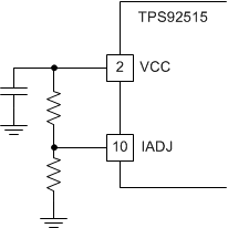
This section describes several analog adjust (IADJ) control methods configurations.
Table 1. IADJ Pin Connection Schematics
| FIGURE | IADJ PIN CONNECTION |
|---|---|
| Figure 17 | IADJ pin tied directly to the VCC pin using the internal 2.4-V clamp. |
| Figure 18 | IADJ pin tied through a voltage divider to the VCC pin allowing a lower peak current sense voltage |
| Figure 19 | IADJ pin tied through a resistor and thermistor divider, implementing thermal foldback function. |
| Figure 20 | IADJ pin is connected to a micro controller. A GPI/GPIO is connected to a filter to create an analog adjust voltage. |
| Figure 21 | IADJ pin connection to implement a soft-start sequence |
| Figure 22 | IADJ pin is connected to a precision reference. This configuration yields the highest accuracy. |
.
 Figure 17.
  Figure 19.
  Figure 21.
  Figure 18.
  Figure 20.
  Figure 22.