SLUSDG2 October 2018 TPS92515AHV-Q1
PRODUCTION DATA.
- 1 Features
- 2 Applications
- 3 Description
- 4 Revision History
- 5 Device Comparison Table
- 6 Pin Configuration and Functions
- 7 Specifications
-
8 Detailed Description
- 8.1 Overview
- 8.2 Functional Block Diagram
- 8.3
Feature Description
- 8.3.1 General Operation
- 8.3.2 Current Sense Comparator
- 8.3.3 OFF Timer
- 8.3.4 OFF-Timer, Shunt FET Dimming or Shunted Output Condition
- 8.3.5 Internal N-channel MOSFET
- 8.3.6 VCC Internal Regulator and Undervoltage Lockout (UVLO)
- 8.3.7 Analog Adjust Input
- 8.3.8 Thermal Protection
- 8.3.9 Junction Temperature Relative Estimation
- 8.3.10 BOOT and BOOT UVLO
- 8.3.11 PWM (UVLO and Enable)
- 8.4 Device Functional Modes
-
9 Application and Implementation
- 9.1 Application Information
- 9.2
Typical Application
- 9.2.1 General Design Procedure
- 9.2.2 Design Requirements
- 9.2.3
Detailed Design Procedure
- 9.2.3.1 Calculating Duty Cycle
- 9.2.3.2 Calculate OFF-Time Estimate
- 9.2.3.3 Calculate OFF-Time Resistor ROFF
- 9.2.3.4 Calculate the Inductance Value
- 9.2.3.5 Calculate the Sense Resistance
- 9.2.3.6 Calculate Input Capacitance
- 9.2.3.7 Verify Peak Current for Inductor Selection
- 9.2.3.8 Calculate Output Capacitance
- 9.2.3.9 Calculate UVLO Resistance Values
- 9.2.4 Application Curves
- 9.3 Dos and Don'ts
- 10Power Supply Recommendations
- 11Layout
- 12Device and Documentation Support
- 13Mechanical, Packaging, and Orderable Information
Package Options
Mechanical Data (Package|Pins)
- DGQ|10
Thermal pad, mechanical data (Package|Pins)
- DGQ|10
Orderable Information
8.3.8.1 Maximum Output Current and Junction Temperature
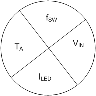
As with all power converter controllers and regulators, practical limits to specification maximums must be considered for each application. For example, it is not possible to operate the TPS92515AHV-Q1 with a switching frequency of 1 MHz, output current of 2 A, at an ambient temperature of 125°C and stay within operating limits. Conversion factors and environment must be considered. This section describes two conversion scenarios with different operating conditions that can result in approximately the same junction temperature. In each case all of the power loss factors combine to develop the device junction temperature.
Figure 24 describes a design with half the output current and a lower switching frequency compared to that shown in Figure 23. However, the design shown in Figure 24 has a higher ambient temperature, higher VIN and an additional external VCC load, resulting in similar junction temperature. Table 2 lists trade-offs and impact on temperature. In general, applications requiring high current (2 A) or a high switching frequency (> 1 MHz) provide reduced maximum ambient temperature levels.

| ILED = 1 A | VIN = 14 V |
| fSW = 500 kHz | TA = 85°C |

| ILED = 500 mA | TA = 125°C |
| fSW = 300 kHz | External VCC load = 500 µA |
| VIN = 60 V |
Table 2. Device Junction Temperature Factors
| FACTOR | AFFECT ON TEMPERATURE AND TRADE-OFFS | |
|---|---|---|
| TA | Ambient temperature | An increase in the ambient temperatre increases the junction temperature by the same amount. |
| VIN | Input voltage | A higher input voltage results in more power developed across the internal regulator resulting in higher internal losses. A higher voltage often yields a larger step-down conversion and lower efficiency. |
| ILED | LED current | A higher LED output current results in higher power (I2R) losses in current carrying elements like the internal MOSFET. |
| IVCC(ext) | External VCC current | Current used to supply additional loads external to the TPS92515AHV-Q1 device draw from the internal regulator. More external current results in an increased junction temperature. When an external source supplies the BOOT current internal power dissipation decreases. |
| fSW | Switching frequency | Each time the internal FET is turned ON and OFF, current must flow from VCC to the gate driver. The current drawn by a switching gate approximately equals the gate charge times the switching frequency. Power loss associated with the switching edge transitions also increase with frequency. |
| η | Efficiency | Switching conversions requiring difficult conversions (small duty cycles) have higher overall losses. These losses increase the overall temperature of the application and the device temperature. |