SLUSD66D September 2019 – February 2021 TPS92520-Q1
PRODUCTION DATA
- 1 Features
- 2 Applications
- 3 Description
- 4 Revision History
- 5 Pin Configuration and Functions
- 6 Specifications
-
7 Detailed Description
- 7.1 Overview
- 7.2 Functional Block Diagram
- 7.3
Feature Description
- 7.3.1 Buck Converter Switching Operation
- 7.3.2 Switching Frequency and Adaptive On-Time Control
- 7.3.3 Minimum On-Time, Off-Time, and Inductor Ripple
- 7.3.4 LED Current Regulation and Error Amplifier
- 7.3.5 Start-up Sequence
- 7.3.6 Analog Dimming and Forced Continuous Conduction Mode
- 7.3.7 External PWM Dimming and Input Undervoltage Lockout (UVLO)
- 7.3.8 Internal PWM Dimming
- 7.3.9 Shunt FET Dimming or Matrix Beam Application
- 7.3.10 Bias Supply
- 7.3.11 Bootstrap Supply
- 7.3.12 ADC
- 7.3.13 Faults and Diagnostics
- 7.3.14 Output Short Circuit Fault
- 7.3.15 Output Open Circuit Fault
- 7.4 Device Functional Modes
- 7.5 Programming
- 7.6
Register Maps
- 7.6.1 Configuration Registers
- 7.6.2 STATUS Registers
- 7.6.3
Device Control Registers
- 7.6.3.1 Thermal Warning Limit (address = 0x06) [reset = 0x8A]
- 7.6.3.2 SLEEP Command (address = 0x07) [reset = 0x00]
- 7.6.3.3 CH1IADJL Control Register (address = 0x08) [reset = 0x00]
- 7.6.3.4 CH1IADJH Control Register (address = 0x09) [reset = 0x00]
- 7.6.3.5 CH2IADJL Control Register (address = 0x0A) [reset = 0x00]
- 7.6.3.6 CH2IADJH Control Register (address = 0x0B) [reset = 0x00]
- 7.6.3.7 PWMDIV Register (address = 0x0C) [reset = 0x04]
- 7.6.3.8 CH1PWML Register (address = 0x0D) [reset = 0x00]
- 7.6.3.9 CH1PWMH Register (address = 0x0E) [reset = 0x00]
- 7.6.3.10 CH2PWML Register (address = 0x0F) [reset = 0x00]
- 7.6.3.11 CH2PWMH Register (address = 0x10) [reset = 0x00]
- 7.6.3.12 CH1TON Register (address = 0x11) [reset = 0x07]
- 7.6.3.13 CH2TON Register (address = 0x12) [reset = 0x07]
- 7.6.4
ADC Measurements
- 7.6.4.1 CH1VIN Measurement (address = 0x13)
- 7.6.4.2 CH1VLED Measurement (address = 0x14)
- 7.6.4.3 CH1VLEDON Measurement (address = 0x15)
- 7.6.4.4 CH1VLEDOFF Measurement (address = 0x16)
- 7.6.4.5 CH2VIN Measurement (address = 0x17)
- 7.6.4.6 CH2VLED Measurement (address = 0x18)
- 7.6.4.7 CH2VLEDON Measurement (address = 0x19)
- 7.6.4.8 CH2VLEDOFF Measurement (address = 0x1A)
- 7.6.4.9 TEMPL Measurement (address = 0x1B)
- 7.6.4.10 TEMPH Measurement (address = 0x1C)
- 7.6.4.11 V5D Measurement (address = 0x1D)
- 7.6.5
Limp-Home Configuration and Command Registers
- 7.6.5.1 LHCFG1 Register (address = 0x1E) [reset =0x00]
- 7.6.5.2 LHCFG2 Register (address = 0x1F) [reset =0x00h]
- 7.6.5.3 LHIL Measurement (address = 0x20)
- 7.6.5.4 LHIH Measurement (address = 0x21)
- 7.6.5.5 LHIFILTL Register (address = 0x22)
- 7.6.5.6 LHIFILTH Register (address = 0x23)
- 7.6.5.7 LH1IADJL Register (address = 0x24) [reset = 0x00]
- 7.6.5.8 LH1IADJH Register (address = 0x25) [reset = 0x00]
- 7.6.5.9 LH2IADJL Register (address = 0x26) [reset = 0x00]
- 7.6.5.10 LH2IADJH Register (address = 0x27) [reset = 0x00]
- 7.6.5.11 LH1PWML Register (address = 0x28) [reset = 0x00]
- 7.6.5.12 LH1PWMH Register (address = 0x29) [reset = 0x00]
- 7.6.5.13 LH2PWML Register (address = 0x2A) [reset = 0x00]
- 7.6.5.14 LH2PWMH Register (address = 0x2B) [reset = 0x00]
- 7.6.5.15 LH1TON Register (address = 0x2C) [reset = 0x07]
- 7.6.5.16 LH2TON Register (address = 0x2D) [reset = 0x07]
- 7.6.6 RESET Register (address = 0x2E) (Write-Only)
-
8 Application and Implementation
- 8.1
Application Information
- 8.1.1 Duty Cycle Consideration
- 8.1.2 Switching Frequency Selection
- 8.1.3 LED Current Set Point
- 8.1.4 Inductor Selection
- 8.1.5 Output Capacitor Selection
- 8.1.6 Input Capacitor Selection
- 8.1.7 Bootstrap Capacitor Selection
- 8.1.8 Compensation Capacitor Selection
- 8.1.9 Input Undervoltage Protection
- 8.1.10 CSN Protection Diode
- 8.2
Typical Application
- 8.2.1
Design Requirements
- 8.2.1.1
Detailed Design Procedure
- 8.2.1.1.1 Calculating Duty Cycle
- 8.2.1.1.2 Calculating Minimum On-Time and Off-Time
- 8.2.1.1.3 Minimum Switching Frequency
- 8.2.1.1.4 LED Current Set Point
- 8.2.1.1.5 Inductor Selection
- 8.2.1.1.6 Output Capacitor Selection
- 8.2.1.1.7 Bootstrap Capacitor Selection
- 8.2.1.1.8 Compensation Capacitor Selection
- 8.2.1.1.9 External Channel Enable and PWM dimming
- 8.2.1.1
Detailed Design Procedure
- 8.2.2 Application Curves
- 8.2.1
Design Requirements
- 8.3 Initialization Setup
- 8.1
Application Information
- 9 Power Supply Recommendations
- 10Layout
- 11Device and Documentation Support
- 12Mechanical, Packaging, and Orderable Information
Package Options
Mechanical Data (Package|Pins)
Thermal pad, mechanical data (Package|Pins)
Orderable Information
7.3.8 Internal PWM Dimming
The TPS92520-Q1 incorporates an internal 10-bit counter to independently configure PWM dimming for each channel. To use the internal PWM, set the CHxINTPWM bit in the SYSCFG1 register. The duty cycle of the internal PWM can be set using a 10-bit value in the CHxPWML and CHxPWMH registers. Since CHxPWM is a 10-bit value, a PWM duty cycle update can require two SPI writes, one to the CHxPWMH and another to the CHxPWML register. In order to prevent transferring unintentional values, the contents of the two registers are only transferred to the CHxPWM counter upon the write to the CHxPWML register. Therefore, to update the PWM duty cycle, it is required to write a value to the CHxPWMH first, and in a consecutive command, write a value to the CHxPWML register. In addition, to avoid corrupting the progress of the current PWM duty cycle, the update from the CHxPWM register to the CHxPWM counter occurs two PWMCLK counts before the end of each PWM period (at the count of 1022).
The clock to the 10-bit PWM counter is set by a 3-bit value in the PWMDIV register. Equation 11 and Equation 12 show the relationship between the PWMCLK and PWM frequency with a 10.8-MHz oscillator, CLKM.
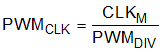
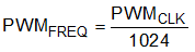
For example, a PWMDIV[2:0] register setting of decimal value 5 sets the division ratio to 24 and results in a PWM frequency of 439 Hz. Refer to Section 7.6.3.7 for more details.
The device can be controlled through the input of the UDIM independent of the internal PWM setting. The signal at the UDIM input is ANDed with the internal PWM to generate a combined output which controls the switching operation. Therefore, each channel can be independently disabled based on the external UDIM signal, even when the device is configured to operate based on internal PWM settings.