SLVSGL7A December 2021 – March 2022 TPS92624-Q1
PRODUCTION DATA
- 1 Features
- 2 Applications
- 3 Description
- 4 Revision History
- 5 Pin Configuration and Functions
- 6 Specifications
-
7 Detailed Description
- 7.1 Overview
- 7.2 Functional Block Diagram
- 7.3
Feature Description
- 7.3.1 Power Supply (SUPPLY)
- 7.3.2 Enable and Shutdown
- 7.3.3 Constant-Current Output and Setting (INx)
- 7.3.4 Thermal Sharing Resistor (OUTx and RESx)
- 7.3.5 PWM Control (PWMx)
- 7.3.6 Supply Control
- 7.3.7 Diagnostics
- 7.3.8 FAULT Bus Output With One-Fails-All-Fail
- 7.3.9 FAULT Table
- 7.3.10 LED Fault Summary
- 7.3.11 IO Pins Inner Connection
- 7.4 Device Functional Modes
- 8 Application and Implementation
- 9 Power Supply Recommendations
- 10Layout
- 11Device and Documentation Support
- 12Mechanical, Packaging, and Orderable Information
Package Options
Mechanical Data (Package|Pins)
- PWP|20
Thermal pad, mechanical data (Package|Pins)
- PWP|20
Orderable Information
5 Pin Configuration and Functions
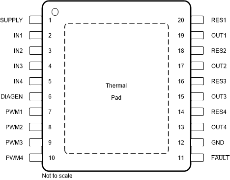
 Figure 5-1 PWP
Package 20-Pin HTSSOP With PowerPAD™ Top View
Figure 5-1 PWP
Package 20-Pin HTSSOP With PowerPAD™ Top ViewTable 5-1 Pin Functions
| PIN | I/O | DESCRIPTION | |
|---|---|---|---|
| NAME | NO. | ||
| SUPPLY | 1 | I | Device power supply |
| IN1 | 2 | I | Current input for channel 1 |
| IN2 | 3 | I | Current input for channel 2 |
| IN3 | 4 | I | Current input for channel 3 |
| IN4 | 5 | I | Current input for channel 4 |
| DIAGEN | 6 | I | Enable pin for LED open-circuit detection to avoid false open diagnostics during low-dropout operation |
| PWM1 | 7 | I | PWM input for OUT1 and RES1 current output ON and OFF control |
| PWM2 | 8 | I | PWM input for OUT2 and RES2 current output ON and OFF control |
| PWM3 | 9 | I | PWM input for OUT3 and RES3 current output ON and OFF control |
| PWM4 | 10 | I | PWM input for OUT4 and RES4 current output ON and OFF control |
| FAULT | 11 | I/O | Fault output, support one-fails–all-fail fault bus |
| GND | 12 | — | Ground |
| OUT4 | 13 | O | Current output for channel 4 |
| RES4 | 14 | O | Current output for channel 4 with external thermal resistor |
| OUT3 | 15 | O | Current output for channel 3 |
| RES3 | 16 | O | Current output for channel 3 with external thermal resistor |
| OUT2 | 17 | O | Current output for channel 2 |
| RES2 | 18 | O | Current output for channel 2 with external thermal resistor |
| OUT1 | 19 | O | Current output for channel 1 |
| RES1 | 20 | O | Current output for channel 1 with external thermal resistor |