SLVSCK5C September 2014 – January 2020 TPS92638-Q1
PRODUCTION DATA.
- 1 Features
- 2 Applications
- 3 Description
- 4 Typical Application Schematic
- 5 Revision History
- 6 Pin Configuration and Functions
- 7 Specifications
- 8 Parameter Measurement Information
- 9 Detailed Description
-
10Application and Implementation
- 10.1 Application Information
- 10.2 Typical Applications
- 11Power Supply Recommendations
- 12Layout
- 13Device and Documentation Support
- 14Mechanical, Packaging, and Orderable Information
Package Options
Mechanical Data (Package|Pins)
- PWP|20
Thermal pad, mechanical data (Package|Pins)
- PWP|20
Orderable Information
9.3.4 Thermal Foldback
The TPS92638-Q1 device integrates thermal shutdown protection to prevent the IC from overheating. In addition, to prevent LEDs from flickering due to rapid thermal changes, the device includes a programmable thermal current foldback feature to reduce power dissipation at high junction temperatures.
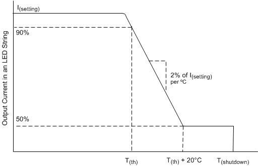
The TPS92638-Q1 device reduces the LED current as the silicon junction temperature of the TPS92638-Q1 device increases (see Figure 35). Mounting the TPS92638-Q1 device on the same thermal substrate as the LEDs allows use of this feature to limit the dissipation of the LEDs. As its junction temperature increases, the TPS92638-Q1 device reduces the regulated current level, thereby reducing the dissipated power in the TPS92638-Q1 and in the LEDs. The current reduction from the 100% level is typically 2% per degree Celsius until the point where the current drops to 50% of the full value, which occurs at T(th) + 20ºC.
 Figure 35. Thermal Foldback
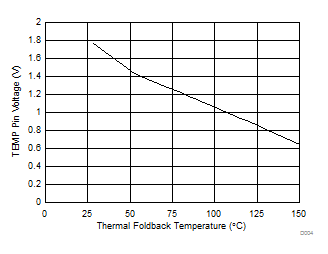
 Above this temperature, the device maintains the current at the 50% current level until the junction temperature reaches the overtemperature shutdown threshold, T(shutdown). Changing the voltage on the TEMP pin adjusts the temperature at which the current reduction begins. With TEMP left open, the definition of thermal monitor activation temperature is the temperature at which the current reduction begins, T(th). The specification of T(th) in the Electrical Characteristics table is at the 90% current level. T(th) increases as the voltage at the TEMP pin, V(TEMP), decreases. Equation 3 provides an approximate calculation of T(th).

 Figure 36. TEMP Pin Voltage vs Thermal Foldback Temperature
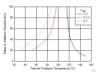
 A resistor connected between TEMP and GND reduces V(TEMP) and increases T(th). A resistor connected between TEMP and a reference supply greater than 1 V increases V(TEMP) and reduces T(th).
 Figure 37. Pullup and Pulldown Resistors vs T(th)
 Figure 37 shows how the nominal value of the thermal monitor activation temperature varies with the voltage at TEMP and with a resistor R(TEMP), either connected to GND or pulled up to 3 V or to 5 V.
In extreme cases, if the junction temperature exceeds the overtemperature limit, T(shutdown), the device disables all regulators. Temperature monitoring continues, and the device re-activates the regulators, when the temperature drops below the specified hysteresis threshold.
Note that it is possible for the TPS92638-Q1 device to transition rapidly between thermal shutdown and normal operation. This can happen if the thermal mass attached to the exposed thermal pad is small and T(th) is too close to the shutdown temperature. The period of oscillation depends on T(th), the dissipated power, the thermal mass of any heatsink present, and the ambient temperature.