DLPS039G December 2015 – July 2024 TPS99000-Q1
PRODUCTION DATA
- 1
- 1 Features
- 2 Applications
- 3 Description
- 4 Pin Configuration and Functions
-
5 Specifications
- 5.1 Absolute Maximum Ratings
- 5.2 ESD Ratings
- 5.3 Recommended Operating Conditions
- 5.4 Thermal Information
- 5.5 Electrical Characteristics—Transimpedance Amplifier Parameters
- 5.6 Electrical Characteristics—Digital to Analog Converters
- 5.7 Electrical Characteristics—Analog to Digital Converter
- 5.8 Electrical Characteristics—FET Gate Drivers
- 5.9 Electrical Characteristics—Photo Comparator
- 5.10 Electrical Characteristics—Voltage Regulators
- 5.11 Electrical Characteristics—Temperature and Voltage Monitors
- 5.12 Electrical Characteristics—Current Consumption
- 5.13 Power-Up Timing Requirements
- 5.14 Power-Down Timing Requirements
- 5.15 Timing Requirements—Sequencer Clock
- 5.16 Timing Requirements—Host and Diagnostic Port SPI Interface
- 5.17 Timing Requirements—ADC Interface
- 5.18 Switching Characteristics
-
6 Detailed Description
- 6.1 Overview
- 6.2 Functional Block Diagram
- 6.3
Feature Description
- 6.3.1
Illumination Control
- 6.3.1.1 Illumination System High Dynamic Range Dimming Overview
- 6.3.1.2 Illumination Control Loop
- 6.3.1.3 Continuous Mode Operation
- 6.3.1.4
Discontinuous Mode Operation
- 6.3.1.4.1 Discontinuous Mode Pulse Width Limit
- 6.3.1.4.2 COMPOUT_LOW Timer in Discontinuous Operation
- 6.3.1.4.3 Dimming Within Discontinuous Operation Range
- 6.3.1.4.4 Multiple Pulse Heights to Increase Bit Depth
- 6.3.1.4.5 TIA Gain Adjustment
- 6.3.1.4.6 Current Limit in Discontinuous Mode
- 6.3.1.4.7 CMODE Big Cap Mode in Discontinuous Operation
- 6.3.2 Over-Brightness Detection
- 6.3.3 Analog to Digital Converter
- 6.3.4 Power Sequencing and Monitoring
- 6.3.5 DMD Mirror Voltage Regulator
- 6.3.6 Low Dropout Regulators
- 6.3.7 System Monitoring Features
- 6.3.8 Communication Ports
- 6.3.1
Illumination Control
- 6.4 Device Functional Modes
- 6.5 Register Maps
- 7 Application and Implementation
- 8 Power Supply Recommendations
- 9 Layout
- 10Device and Documentation Support
- 11Revision History
- 12Mechanical, Packaging, and Orderable Information
Package Options
Mechanical Data (Package|Pins)
- PZP|100
Thermal pad, mechanical data (Package|Pins)
- PZP|100
Orderable Information
6.3.1.4 Discontinuous Mode Operation
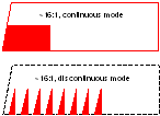
Discontinuous mode is used to achieve lower dimming levels. It replaces the constant block of light during a bit slice with a series of light pulses of controlled amplitude, as illustrated in Figure 6-15. The number of pulses is controlled by the DLPC23x-Q1 software.
 Figure 6-15 Comparison of Continuous and Discontinuous Operation at Equivalent Brightness
Figure 6-15 is an example diagram showing the Discontinuous Mode signals generating eight pulses that are equivalent in brightness.
In discontinuous mode, the controller produces discrete pulses of light with fixed off times between pulses. The amount of light that these pulses produce can be precisely controlled to reach low dimming levels. Two control loops are used to create uniform light pulses:
- Peak current limit loop to create a desired current level in the inductor before it flows through the LED.
- Photo feedback loop to terminate each pulse when the desired light pulse level is achieved.
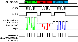
 Figure 6-16 Discontinuous Operation DLPC23x-Q1 to TPS99000-Q1 Signals
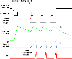
 Figure 6-17 Discontinuous Mode Operation Inductor Current/LED Voltage
Discontinuous mode consists of a series of triangular pulses of light. The DLPC23x-Q1 is in charge of requesting and counting the total number of pulses. A bit slice begins with the low resistance shunt enable (S_EN1) on, and with an RGB color selected. Then DLPC23x-Q1 asserts D_EN. This causes the TPS99000-Q1 to turn on the LED current drive (DRV_EN) and the system charges the inductor into the low resistance shunt until the peak current limit (as programmed with ILIM DAC) is reached. Then after a programmable amount of time the DLPC23x-Q1 drives S_EN low, forcing inductor current to flow through the selected LED.
The TPS99000-Q1 detects the falling edge of S_EN from the DLPC23x-Q1 and issues an on/off/on toggle of the DRV_EN signal. This allows current to flow through the inductor and increases the voltage at the LED anode. When the LED forward voltage is achieved, it begins to emit light. Once the photo feedback loop (TIA, photo feedback comparator, photo feedback DAC) senses the desired light threshold has been crossed, the S_EN1 signal is re-asserted high, and the light pulse is terminated.
The COMPOUT signal going low indicates to the DLPC23x-Q1 that the pulse has been completed. The DLPC23x-Q1 immediately sets S_EN output high (which sets TPS99000-Q1 output S_EN1 high), then waits for a programmable length of time. After that period of time, the DLPC23x-Q1 will decide either to drive D_EN low and wait for the next bit slice or issue a request for a new pulse by placing the S_EN output low. When S_EN output is placed low, the TPS99000-Q1 places S_EN1 low (forcing current through LED) and toggles DRV_EN to request a new peak limit current pulse cycle. This process repeats until the correct number of pulses for the given bit slice have been completed.
In very low brightness operation, the TPS99000-Q1 SYNC (LM3409 COFF) timer is disabled. As a result, DRV_EN is only toggled at the beginning of each light pulse. This synchronizes the inductor and LED current. This synchronization keeps LED pulse heights very consistent from one video frame to the next, preventing flicker.