DLPS039G December 2015 – July 2024 TPS99000-Q1
PRODUCTION DATA
- 1
- 1 Features
- 2 Applications
- 3 Description
- 4 Pin Configuration and Functions
-
5 Specifications
- 5.1 Absolute Maximum Ratings
- 5.2 ESD Ratings
- 5.3 Recommended Operating Conditions
- 5.4 Thermal Information
- 5.5 Electrical Characteristics—Transimpedance Amplifier Parameters
- 5.6 Electrical Characteristics—Digital to Analog Converters
- 5.7 Electrical Characteristics—Analog to Digital Converter
- 5.8 Electrical Characteristics—FET Gate Drivers
- 5.9 Electrical Characteristics—Photo Comparator
- 5.10 Electrical Characteristics—Voltage Regulators
- 5.11 Electrical Characteristics—Temperature and Voltage Monitors
- 5.12 Electrical Characteristics—Current Consumption
- 5.13 Power-Up Timing Requirements
- 5.14 Power-Down Timing Requirements
- 5.15 Timing Requirements—Sequencer Clock
- 5.16 Timing Requirements—Host and Diagnostic Port SPI Interface
- 5.17 Timing Requirements—ADC Interface
- 5.18 Switching Characteristics
-
6 Detailed Description
- 6.1 Overview
- 6.2 Functional Block Diagram
- 6.3
Feature Description
- 6.3.1
Illumination Control
- 6.3.1.1 Illumination System High Dynamic Range Dimming Overview
- 6.3.1.2 Illumination Control Loop
- 6.3.1.3 Continuous Mode Operation
- 6.3.1.4
Discontinuous Mode Operation
- 6.3.1.4.1 Discontinuous Mode Pulse Width Limit
- 6.3.1.4.2 COMPOUT_LOW Timer in Discontinuous Operation
- 6.3.1.4.3 Dimming Within Discontinuous Operation Range
- 6.3.1.4.4 Multiple Pulse Heights to Increase Bit Depth
- 6.3.1.4.5 TIA Gain Adjustment
- 6.3.1.4.6 Current Limit in Discontinuous Mode
- 6.3.1.4.7 CMODE Big Cap Mode in Discontinuous Operation
- 6.3.2 Over-Brightness Detection
- 6.3.3 Analog to Digital Converter
- 6.3.4 Power Sequencing and Monitoring
- 6.3.5 DMD Mirror Voltage Regulator
- 6.3.6 Low Dropout Regulators
- 6.3.7 System Monitoring Features
- 6.3.8 Communication Ports
- 6.3.1
Illumination Control
- 6.4 Device Functional Modes
- 6.5 Register Maps
- 7 Application and Implementation
- 8 Power Supply Recommendations
- 9 Layout
- 10Device and Documentation Support
- 11Revision History
- 12Mechanical, Packaging, and Orderable Information
Package Options
Mechanical Data (Package|Pins)
- PZP|100
Thermal pad, mechanical data (Package|Pins)
- PZP|100
Orderable Information
6.3.1.4.4 Multiple Pulse Heights to Increase Bit Depth
With the TPS99000-Q1, up to four sets of photo feedback threshold settings are supported within a given sequence. This is useful in a discontinuous operation to create smaller sub-LSB bits (bits that are smaller than the normal LSB).
The LED_SEL(3:0) lines are encoded to include group information as well as color selection (and blanking current selection).
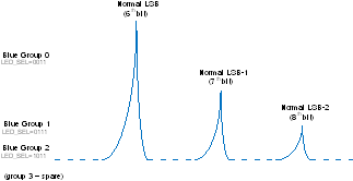
Each group can be defined to determine different behaviors for specific color bits. For example, Group 0 can be used for LSB, and Group 1 can be used to create LSB-1.
| LED_SEL(3:0) | NAME | ACTION |
|---|---|---|
| "0000" | OFF | Driver Disabled Mode S_EN1 forced high RGB selects low |
| "0100" | R BLANKING | LED_SEL(1:0) - "00"=blanking LED_SEL(3:2): "01"=red "10"=green "11"=blue |
| "1000" | G BLANKING | |
| "1100" | B BLANKING | |
| "0001" | GRP0 RED | Driver Enabled Mode: LED_SEL(3:2) - Define Group: '00' - Group 0 '01' - Group 1 '10' - Group 2 '11' - Group 3 LED_SEL(1:0): "01" - red "10" - green "11" - blue |
| "0010" | GRP0 GREEN | |
| "0011" | GRP0 BLUE | |
| "0101" | GRP1 RED | |
| "0110" | GRP1 GREEN | |
| "0111" | GRP1 BLUE | |
| "1001" | GRP2 RED | |
| "1010" | GRP2 GREEN | |
| "1011" | GRP2 BLUE | |
| "1101" | GRP3 RED | |
| "1110" | GRP3 GREEN | |
| "1111" | GRP3 BLUE |
The group1-3 RGB selections may be used to create fractional LSBs in the sequence, as illustrated in Figure 6-23.
 Figure 6-23 Extended LSB Bit Depth in Discontinuous Operation
This feature, combined with the ability to make smaller absolute-size light pulses, provides a method to extend the practical bit depth limit from the typical 6 bits per color, as is the case in legacy systems, to 7 or 8 bits with TPS99000-Q1/DLPC23x-Q1 second-generation systems.