SNVSC83B September 2022 – February 2023 TPSM365R3 , TPSM365R6
PRODUCTION DATA
- 1 Features
- 2 Applications
- 3 Description
- 4 Revision History
- 5 Description (continued)
- 6 Device Comparison Table
- 7 Pin Configuration and Functions
-
8 Specifications
- 8.1 Absolute Maximum Ratings
- 8.2 ESD Ratings
- 8.3 Recommended Operating Conditions
- 8.4 Thermal Information
- 8.5 Electrical Characteristics
- 8.6 System Characteristics
- 8.7 Typical Characteristics
- 8.8 Typical Characteristics: VIN = 12 V
- 8.9 Typical Characteristics: VIN = 24 V
- 8.10 Typical Characteristics: VIN = 48 V
-
9 Detailed Description
- 9.1 Overview
- 9.2 Functional Block Diagram
- 9.3
Feature Description
- 9.3.1 Input Voltage Range
- 9.3.2 Output Voltage Selection
- 9.3.3 Input Capacitors
- 9.3.4 Output Capacitors
- 9.3.5 Enable, Start-Up, and Shutdown
- 9.3.6 External CLK SYNC (with MODE/SYNC)
- 9.3.7 Switching Frequency (RT)
- 9.3.8 Power-Good Output Operation
- 9.3.9 Internal LDO, VCC UVLO, and BIAS Input
- 9.3.10 Bootstrap Voltage and VBOOT-UVLO (BOOT Terminal)
- 9.3.11 Spread Spectrum
- 9.3.12 Soft Start and Recovery from Dropout
- 9.3.13 Overcurrent Protection (OCP)
- 9.3.14 Thermal Shutdown
- 9.4 Device Functional Modes
-
10Application and Implementation
- 10.1 Application Information
- 10.2
Typical Application
- 10.2.1
600-mA and 300-mA Synchronous Buck Regulator for
Industrial Applications
- 10.2.1.1 Design Requirements
- 10.2.1.2
Detailed Design Procedure
- 10.2.1.2.1 Custom Design With WEBENCH® Tools
- 10.2.1.2.2 Output Voltage Setpoint
- 10.2.1.2.3 Switching Frequency Selection
- 10.2.1.2.4 Input Capacitor Selection
- 10.2.1.2.5 Output Capacitor Selection
- 10.2.1.2.6 VCC
- 10.2.1.2.7 CFF Selection
- 10.2.1.2.8 Power-Good Signal
- 10.2.1.2.9 Maximum Ambient Temperature
- 10.2.1.2.10 Other Connections
- 10.2.1.3 Application Curves
- 10.2.1
600-mA and 300-mA Synchronous Buck Regulator for
Industrial Applications
- 10.3 Power Supply Recommendations
- 10.4 Layout
- 11Device and Documentation Support
- 12Mechanical, Packaging, and Orderable Information
Package Options
Mechanical Data (Package|Pins)
- RDN|11
Thermal pad, mechanical data (Package|Pins)
Orderable Information
10.2.1.3 Application Curves
Unless otherwise indicated, VIN = 24 V, VOUT = 5 V, IOUT = 0.5 A, and FSW = 1 MHz
| VIN = 24 V | VOUT = 5 V |
| VIN = 24 V | VOUT = 3.3 V | FSW = 1 MHz |
| COUT = 2 × 22 µF |
| VIN = 24 V | VOUT = 5 V | FSW = 1 MHz |
| COUT = 2 × 22 µF |
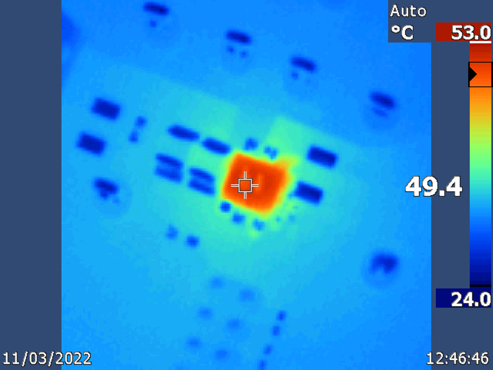
 Figure 10-9 Thermal Image, VIN = 24 V, VOUT = 12 V,
FSW = 2.2 MHz, IOUT = 0.6 A (Standard EVM and
BOM)
Figure 10-9 Thermal Image, VIN = 24 V, VOUT = 12 V,
FSW = 2.2 MHz, IOUT = 0.6 A (Standard EVM and
BOM)| VIN = 24 V | VOUT = 5 V | fSW = 1 MHz |
| Load = 500 mA |
| VIN = 24 V | VOUT = 5 V | fSW = 1 MHz |
| Load = 500 mA |
| VIN = 24 V | VOUT = 5 V |
| VIN = 24 V | VOUT = 3.3 V | FSW = 1 MHz |
| COUT = 2 × 22 µF |
| VIN = 24 V | VOUT = 5 V | F SW = 1 MHz |
| COUT = 2 × 22 µF |
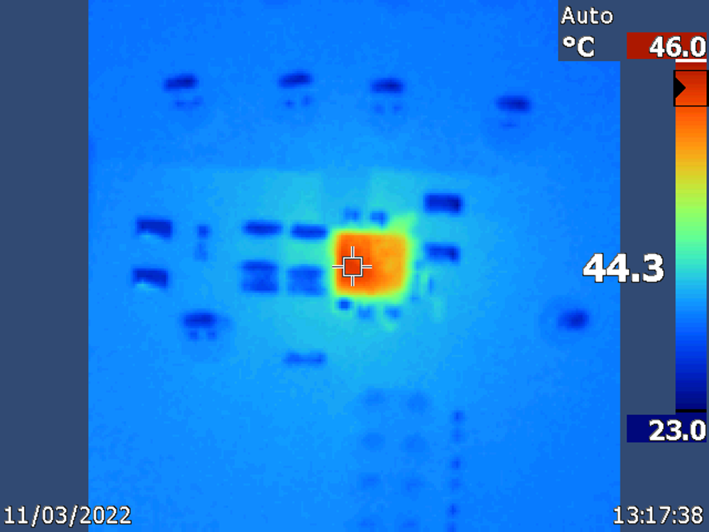
 Figure 10-10 Thermal Image, VIN = 24 V, VOUT = 5 V, FSW
= 1 MHz, IOUT = 0.6 A (Standard EVM and BOM)
Figure 10-10 Thermal Image, VIN = 24 V, VOUT = 5 V, FSW
= 1 MHz, IOUT = 0.6 A (Standard EVM and BOM)| VIN = 24 V | VOUT = 5 V | fSW = 1 MHz |
| Load = 500 mA |