SLVSG72 September 2021 TPSM560R6H
PRODUCTION DATA
- 1 Features
- 2 Applications
- 3 Description
- 4 Revision History
- 5 Pin Configuration and Functions
-
6 Specifications
- 6.1 Absolute Maximum Ratings
- 6.2 ESD Ratings
- 6.3 Recommended Operating Conditions
- 6.4 Thermal Information
- 6.5 Electrical Characteristics
- 6.6 Typical Characteristics (VIN = 12 V)
- 6.7 Typical Characteristics (VIN = 24 V)
- 6.8 Typical Characteristics (VIN = 48 V)
- 6.9 Typical Characteristics (VIN = 60 V)
- 7 Detailed Description
- 8 Applications and Implementation
- 9 Power Supply Recommendations
- 10Layout
- 11Device and Documentation Support
- 12Mechanical, Packaging, and Orderable Information
Package Options
Mechanical Data (Package|Pins)
- RDA|15
Thermal pad, mechanical data (Package|Pins)
Orderable Information
7.3.3 Minimum Output Capacitance
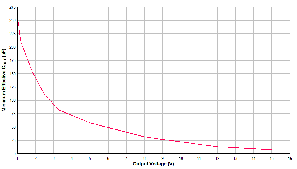
The TPSM560R6H requires a minimum amount of ceramic output capacitance for stability, depending on the output voltage setting. Figure 7-2 shows the amount of required output capacitance, which is also the amount of effective capacitance. The effects of DC bias and temperature variation must be considered when using ceramic capacitance. For ceramic capacitors, the package size, voltage rating, and dielectric material contribute to the differences between the standard rated value and the actual effective value of the capacitance. Additional output capacitance above the minimum can be added to reduce output voltage ripple and to improve transient response. When adding additional capacitance above the minimum, the capacitance can be ceramic type, low-ESR polymer type, or a combination of the two.
 Figure 7-2 Minimum Required Output
Capacitance