SLUSDV8B November   2020  – March 2021 TPSM5D1806

PRODUCTION DATA  

  1. Features
  2. Applications
  3. Description
  4. Revision History
  5. Pin Configuration and Functions
  6. Specifications
    1. 6.1 Absolute Maximum Ratings
    2. 6.2 ESD Ratings
    3. 6.3 Recommended Operating Conditions
    4. 6.4 Thermal Information
    5. 6.5 Electrical Characteristics
    6. 6.6 Typical Characteristics (VIN = 12 V)
    7. 6.7 Typical Characteristics (VIN = 5 V)
  7. Detailed Description
    1. 7.1 Overview
    2. 7.2 Functional Block Diagram
    3. 7.3 Feature Description
      1. 7.3.1  Adjustable Output Voltage
      2. 7.3.2  Frequency Selection
        1. 7.3.2.1 Synchronization
        2. 7.3.2.2 Allowable Switching Frequency
      3. 7.3.3  Minimum and Maximum Input Voltage
      4. 7.3.4  Recommended Settings
      5. 7.3.5  Device Mode Configuration
        1. 7.3.5.1 MODE1 (Operating Mode and Phase Position)
        2. 7.3.5.2 MODE2 (Setting the Switching Frequency)
      6. 7.3.6  Input Capacitors
      7. 7.3.7  Minimum Required Output Capacitance
      8. 7.3.8  Ambient Temperature Versus Total Power Dissipation
      9. 7.3.9  Remote Sense
      10. 7.3.10 Enable (EN) and Under Voltage Lockout (UVLO)
      11. 7.3.11 Soft Start
      12. 7.3.12 Power Good
      13. 7.3.13 Safe Start-up into Pre-Biased Outputs
      14. 7.3.14 BP5
      15. 7.3.15 Overcurrent Protection
      16. 7.3.16 Thermal Shutdown
    4. 7.4 Device Functional Modes
      1. 7.4.1 Active Mode
      2. 7.4.2 Shutdown Mode
  8. Application and Implementation
    1. 8.1 Application Information
    2. 8.2 Typical Application (Dual Outputs)
      1. 8.2.1 Design Requirements
      2. 8.2.2 Detailed Design Procedure
        1. 8.2.2.1 Custom Design With WEBENCH® Tools
        2. 8.2.2.2 Output Voltage Setpoint
        3. 8.2.2.3 Input Capacitors
        4. 8.2.2.4 Output Capacitor Selection
      3. 8.2.3 Typical Application (Paralleled Outputs)
        1. 8.2.3.1 Design Requirements
        2. 8.2.3.2 Detailed Design Procedure
          1. 8.2.3.2.1 Output Voltage Setpoint
          2. 8.2.3.2.2 Input Capacitors
          3. 8.2.3.2.3 Output Capacitor Selection
  9. Power Supply Recommendations
  10. 10Layout
    1. 10.1 Layout Guidelines
    2. 10.2 Layout Examples
      1. 10.2.1 Package Specifications
      2. 10.2.2 EMI
  11. 11Device and Documentation Support
    1. 11.1 Device Support
      1. 11.1.1 Development Support
        1. 11.1.1.1 Custom Design With WEBENCH® Tools
    2. 11.2 Receiving Notification of Documentation Updates
    3. 11.3 Support Resources
    4. 11.4 Trademarks
    5. 11.5 Electrostatic Discharge Caution
    6. 11.6 Glossary
  12. 12Mechanical, Packaging, and Orderable Information

Package Options

Mechanical Data (Package|Pins)
Thermal pad, mechanical data (Package|Pins)
Orderable Information

Typical Characteristics (VIN = 5 V)

TA = 25°C unless otherwise noted.

GUID-20210119-CA0I-58PX-WSLZ-8TCDWTXKM4M6-low.gifFigure 6-8 Efficiency vs Output Current
GUID-20210119-CA0I-WWSK-S3JT-BCMBHCRRFZSC-low.gif
Refer to Table 7-1
Figure 6-10 Maximum Output Current
GUID-20201118-CA0I-Q9PW-CTQX-FH08FTHMMTVS-low.gif
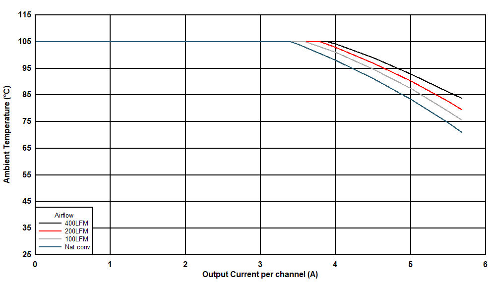
Fsw = 1.5 MHz Dual 1.2-V outputs IOUT1 = IOUT2
Figure 6-12 Safe Operating Area (VOUT = 1.2 V)
GUID-20210119-CA0I-S51C-BXSF-K3VRS18VCTW1-low.gif
Fsw = 2.0 MHz Dual 3.3-V outputs IOUT1 = IOUT2
Figure 6-14 Safe Operating Area (VOUT = 3.3 V)
GUID-20210119-CA0I-XMQR-VQZF-VCZSRGVJDXZJ-low.gifFigure 6-9 Power Dissipation vs Output Current
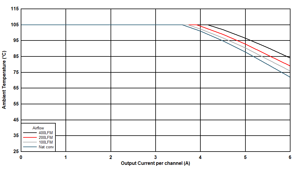
GUID-20210119-CA0I-L4Z1-GZGV-LKS8NQXPKQCF-low.gif
Fsw = 1.0 MHz Dual 0.8-V outputs IOUT1 = IOUT2
Figure 6-11 Safe Operating Area (VOUT = 0.8 V)
GUID-20210119-CA0I-VKSJ-6WHL-Q5QQCSDPFQDQ-low.gif
Fsw = 1.5 MHz Dual 1.8-V outputs IOUT1 = IOUT2
Figure 6-13 Safe Operating Area (VOUT = 1.8 V)