SLVSHK8A December 2023 – June 2024 TPSM64404 , TPSM64406 , TPSM64406E
PRODUCTION DATA
- 1
- 1 Features
- 2 Applications
- 3 Description
- 4 Device Comparison Table
- 5 Pin Configuration and Functions
- 6 Specifications
-
7 Detailed Description
- 7.1 Overview
- 7.2 Functional Block Diagram
- 7.3
Feature Description
- 7.3.1 Input Voltage Range (VIN1, VIN2)
- 7.3.2 Enable EN Pin and Use as VIN UVLO
- 7.3.3 CONFIG Device Configuration Pin
- 7.3.4 Adjustable Switching Frequency
- 7.3.5 Spread Spectrum
- 7.3.6 Adjustable Output Voltage (FB)
- 7.3.7 Input Capacitors
- 7.3.8 Output Capacitors
- 7.3.9 SYNC Allows Clock Synchronization and Mode Selection
- 7.3.10 Power-Good Output Voltage Monitoring
- 7.3.11 Bias Supply Regulator (VCC, VOSNS)
- 7.3.12 Overcurrent Protection (OCP)
- 7.3.13 Thermal Shutdown
- 7.4 Device Functional Modes
-
8 Applications and Implementation
- 8.1 Application Information
- 8.2 Typical Applications
- 8.3 Power Supply Recommendations
- 8.4 Layout
- 9 Device and Documentation Support
- 10Revision History
- 11Mechanical, Packaging, and Orderable Information
Package Options
Mechanical Data (Package|Pins)
- RCH|28
Thermal pad, mechanical data (Package|Pins)
Orderable Information
7.3.9 SYNC Allows Clock Synchronization and Mode Selection
The SYNC pin can be used to select forced pulse width modulation (FPWM) or pulse frequency modulation (PFM). In FPWM the switching frequency remains constant at lighter output currents. In PFM the low-side FET is turned off when the inductor current goes negative and the frequency is reduced to improve efficiency under light-load conditions. Connect SYNC to AGND to enable PFM. Connect SYNC to VCC to operate the TPSM6440X in FPWM mode with continuous conduction at light loads.
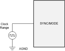
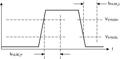
The SYNC pin can also be used to synchronize the internal oscillator to an external clock. When synchronized to an external clock, the TPSM6440X operates in FPWM. The internal oscillator can be synchronized to a positive edge into the SYNC pin. The coupled edge voltage at the SYNC pin must exceed the SYNC amplitude threshold of VSYNCDH to trip the internal synchronization pulse detector. The minimum SYNC rising pulse and falling pulse durations must be longer than tPULSE_H and tPULSE_L respectively. The TPSM6440X switching action can be synchronized to an external clock from 200 kHz to 2.2 MHz. When synchronizing to an external clock, the RT pin must be used to set the internal frequency to a value close to that of the external clock. This action prevents large frequency changes in the event of loss of synchronization. This action is also used to set the slope compensation for secondary devices.
In single-output two-phase operation, the PG2/SYNC-OUT terminal of the primary can be left floating as clock information is shared internally.
In single-output four-phase operation, the PG2/SYNC-OUT terminal of the primary must be connected to the SYNC pin of the secondary to clock all four phases 90 degrees out of phase.
In single-output six-phase operation, the PG2/SYNC-OUT terminal of the primary must be connected to the SYNC pin of the secondary device. The PG2/SYNC-OUT terminal of the secondary must be connected to the SYNC pin of the tertiary device. In this way, the devices operate all six phases 60 degrees out of phase.
 Figure 7-7 Typical Implementation Allowing Synchronization Using the SYNC/MODE Pin
| This image shows the conditions needed for detection of a synchronization signal. |