SLUSDN6B September 2019 – July 2024 TPSM82810 , TPSM82813
PRODMIX
- 1
- 1 Features
- 2 Applications
- 3 Description
- 4 Device Comparison Table
- 5 Pin Configuration and Functions
- 6 Specifications
- 7 Parameter Measurement Information
- 8 Detailed Description
- 9 Application and Implementation
- 10Device and Documentation Support
- 11Revision History
- 12Mechanical, Packaging, and Orderable Information
Package Options
Mechanical Data (Package|Pins)
- SIL|14
Thermal pad, mechanical data (Package|Pins)
Orderable Information
8.3.3 COMP/FSET
This pin sets two different parameters independently:
- Internal compensation settings for the control loop (three settings available)
- The switching frequency in PWM mode from 1.8MHz to 4MHz
A resistor from COMP/FSET to GND changes the compensation as well as the switching frequency. The change in compensation adapts the device to different values of output capacitance. The resistor must be placed close to the pin to keep the parasitic capacitance on the pin to a minimum. The compensation setting is set after enabling the converter, so a change in the resistor during operation only has an effect on the switching frequency but not on the compensation.
To save external components, the pin can also be directly tied to VIN or GND to set a pre-defined switching frequency and compensation. Do not leave the pin floating.
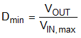
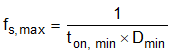
The switching frequency must be selected based on the maximum input voltage and the output voltage to meet the specifications for the minimum on-time. Using VIN = 5.5V and VOUT = 1.1V as an example, the minimum duty cycle given with Equation 1 is 0.2, which results in a maximum switching frequency of 2.67MHz according to Equation 2.
The compensation range has to be chosen based on the minimum effective capacitance used. The capacitance can be increased from the minimum value as given in Table 8-1 up to the maximum of 470µF in all of the three compensation ranges. If the capacitance of an output changes during operation, for example, when load switches are used to connect or disconnect parts of the circuitry, the compensation has to be chosen for the minimum capacitance on the output. With large output capacitance, the compensation must be done based on that large capacitance to get the best load transient response. Compensating for large output capacitance but placing less capacitance on the output can lead to instability.
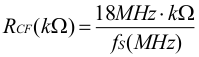
The switching frequency for the different compensation setting is determined by the following equations.
For compensation (comp) setting 1:
For compensation (comp) setting 2:

For compensation (comp) setting 3:
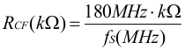
| COMPENSATION | RCF | SWITCHING FREQUENCY | MINIMUM OUTPUT CAPACITANCE FOR VOUT < 1V | MINIMUM OUTPUT CAPACITANCE FOR 1V ≤ VOUT < 3.3V | MINIMUM OUTPUT CAPACITANCE FOR VOUT ≥ 3.3V |
|---|---|---|---|---|---|
| for smallest output capacitance (comp setting 1) | 10kΩ ... 4.5kΩ | 1.8MHz (10kΩ) ... 4MHz (4.5kΩ) according to Equation 3 | 53µF | 32µF | 27µF |
| for medium output capacitance (comp setting 2) | 33kΩ ... 15kΩ | 1.8MHz (33kΩ) ... 4MHz (15kΩ) according to Equation 4 | 100µF | 60µF | 50µF |
| for large output capacitance (comp setting 3) | 100kΩ ... 45kΩ | 1.8MHz (100kΩ) ... 4MHz (45kΩ) according to Equation 5 | 200µF | 120µF | 100µF |
| for smallest output capacitance (comp setting 1) | tied to GND | internally fixed 2.25MHz | 53µF | 32µF | 27µF |
| for large output capacitance (comp setting 3) | tied to VIN | internally fixed 2.25MHz | 200µF | 120µF | 100µF |
Refer to Section 9.2.2.5 for further details on the output capacitance required depending on the output voltage. All values are the effective value of capacitance.
A too high resistor value for RCF is read as "tied to VIN", and a value below the lowest range as "tied to GND". The minimum output capacitance in Table 8-1 is for capacitors close to the output of the device. If the capacitance is distributed, a lower compensation setting can be required.