SLUSDN6B September   2019  – July 2024 TPSM82810 , TPSM82813

PRODMIX  

  1.   1
  2. Features
  3. Applications
  4. Description
  5. Device Comparison Table
  6. Pin Configuration and Functions
  7. Specifications
    1. 6.1 Absolute Maximum Ratings
    2. 6.2 ESD Ratings
    3. 6.3 Recommended Operating Conditions
    4. 6.4 Thermal Information
    5. 6.5 Thermal Information
    6. 6.6 Electrical Characteristics
    7. 6.7 Typical Characteristics
  8. Parameter Measurement Information
    1. 7.1 Schematic
  9. Detailed Description
    1. 8.1 Overview
    2. 8.2 Functional Block Diagram
    3. 8.3 Feature Description
      1. 8.3.1 Precise Enable (EN)
      2. 8.3.2 Output Discharge
      3. 8.3.3 COMP/FSET
      4. 8.3.4 MODE/SYNC
      5. 8.3.5 Spread Spectrum Clocking (SSC) - TPSM8281xS
      6. 8.3.6 Undervoltage Lockout (UVLO)
      7. 8.3.7 Power-Good Output (PG)
      8. 8.3.8 Thermal Shutdown
    4. 8.4 Device Functional Modes
      1. 8.4.1 Pulse Width Modulation (PWM) Operation
      2. 8.4.2 Power Save Mode Operation (PFM/PWM)
      3. 8.4.3 100% Duty-Cycle Operation
      4. 8.4.4 Current Limit and Short Circuit Protection
      5. 8.4.5 Soft Start / Tracking (SS/TR)
  10. Application and Implementation
    1. 9.1 Application Information
    2. 9.2 Typical Application
      1. 9.2.1 Design Requirements
      2. 9.2.2 Detailed Design Procedure
        1. 9.2.2.1 Custom Design With WEBENCH® Tools
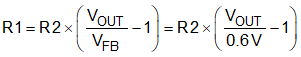
        2. 9.2.2.2 Programming the Output Voltage
        3. 9.2.2.3 Feedforward capacitor
        4. 9.2.2.4 Input Capacitor
        5. 9.2.2.5 Output Capacitor
      3. 9.2.3 Application Curves
    3. 9.3 System Examples
      1. 9.3.1 Voltage Tracking
      2. 9.3.2 Synchronizing to an External Clock
    4. 9.4 Power Supply Recommendations
    5. 9.5 Layout
      1. 9.5.1 Layout Guidelines
      2. 9.5.2 Layout Example
        1. 9.5.2.1 Thermal Consideration
  11. 10Device and Documentation Support
    1. 10.1 Device Support
      1. 10.1.1 Third-Party Products Disclaimer
      2. 10.1.2 Custom Design With WEBENCH® Tools
    2. 10.2 Documentation Support
      1. 10.2.1 Related Documentation
    3. 10.3 Receiving Notification of Documentation Updates
    4. 10.4 Support Resources
    5. 10.5 Trademarks
    6. 10.6 Electrostatic Discharge Caution
    7. 10.7 Glossary
  12. 11Revision History
  13. 12Mechanical, Packaging, and Orderable Information

Package Options

Mechanical Data (Package|Pins)
Thermal pad, mechanical data (Package|Pins)
Orderable Information

Programming the Output Voltage

The output voltage of the TPSM8281x is adjustable. Choose resistors R1 and R2 to set the output voltage within a range of 0.6V to 5.5V according to Equation 10. To keep the feedback (FB) net robust from noise, set R2 equal to or lower than 100kΩ to have at least 6µA of current in the voltage divider. Lower values of FB resistors achieve better noise immunity, and lower light load efficiency, as explained in the Design Considerations for a Resistive Feedback Divider in a DC/DC Converter analog design journal.

Equation 10. TPSM82810 TPSM82813